
Page 311 - Sami Franssila Introduction to Microfabrication
P. 311
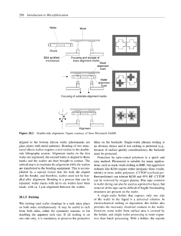
290 Introduction to Microfabrication


                              Wafer             Mask


                              Chuck

                           BSA splitfield  Focusing and storage of
                            microscope      mask alignment marks
                                                            Mask
                                                           alignment
                                                            mark


                                                             Wafer
                                                           alignment
                                                             mark


                                     Focusing of substrate alignment marks


                                                Alignment
            Figure 28.2 Double-side alignment. Figure courtesy of Suss Microtech GmbH

            aligned to the bottom silicon wafer (photomasks are  films on the backside. Single-wafer plasma etching is
            glass plates with metal patterns). Bonding of two struc-  an obvious choice and if wet etching is preferred (e.g.,
            tured silicon wafers requires a tool similar to the double-  because of surface quality considerations), the backside
            side lithography system. Alignment marks on the first  must be protected.
            wafer are registered, the second wafer is aligned to those  Protection by spin-coated polymers is a quick and
            marks and the wafers are then brought to contact. The  easy method. Photoresist is suitable for many applica-
            critical step is to maintain the alignment while the wafers  tions, such as mask oxide etching in BHF, but aggressive
            are transferred to the bonding equipment. This is accom-  etchants like KOH require either inorganic films (oxide,
            plished by a special fixture that fits both the aligner  nitride) or more stable polymers. CYTOP (cyclized per-
            and the bonder, and therefore, wafers need not be han-  fluoropolymer) can tolerate KOH and 49% HF. CYTOP
            dled after alignment. Bonding is a process that can be  can be removed by oxygen plasma. Blue tape common
            repeated: wafer stacks with up to six wafers have been  in wafer dicing can also be used as a protective layer, but
            made, with ca. 1 µm alignment between the wafers.  removal of the tape can be difficult if fragile freestanding
                                                         structures are present on the wafer.
                                                           A single-wafer holder that exposes only one side
            28.1.5 Etching
                                                         of the wafer to the liquid is a universal solution. In
            Wet etching (and wafer cleaning) in a tank takes place  electrochemical etching or deposition, this holder also
            on both sides simultaneously. It may be useful to etch  provides the necessary electrical contacts to the wafer.
            from both sides, either for symmetry reasons, or for  However, some wafer front surface area is covered by
            doubling the apparent etch rate. If all etching is on  the holder, and single-wafer processing is more expen-
            one side only, it is mandatory to preserve the protective  sive than batch processing. With a holder, the topside