
Page 316 - Sami Franssila Introduction to Microfabrication
P. 316
MEMS Process Integration 295
Table 28.4 Main features of anisotropic wet etching
– Very accurate dimensional control by crystal
plane–dependent etching
– Structural shapes limited by crystal plane–dependent
etching
◦
– Accurate 45 , 54.7 , 70.5 or 90 sidewalls
◦
◦
◦
– Smooth and well-defined surfaces
– ca. 4–8 hours for through-wafer etching for a single
Figure 28.8 Conventional and micromachined 3D silicon wafer
shadow masks compared. Redrawn from Brugger, J. et al. – ca. 4–8 hours for through-wafer etching for a batch
(1999), by permission of Elsevier of 25 wafers
– Etches both sides, protection needed on backside
– Etches both sides, symmetric structures can be made
28.5 DRIE VERSUS ANISOTROPIC WET in a single etch step
ETCHING
– Aggressive to metals and many other materials
Both plasma etching (RIE/DRIE) and wet etching have – Limited selection of mask materials, thick oxide and
their advantages (Tables 28.3 and 28.4), and in many LPCVD nitride standard ++
applications, both etching techniques are mandatory. – Many etch-stop mechanisms available: boron p ,
pn-junction, SOI BOX
The decision in favour of either technique depends not
only on technological factors such as etched shape, side-
wall angle or surface quality, but also on practical issues
such as etch rate, backside protection or equipment 1
availability.
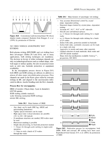
In the micropipette process shown in Figure 28.9,
both DRIE and KOH etching are utilized, in addition to
almost all other major microfabrication processes. Flow 2
channels are made in the Pyrex glass wafer by isotropic
etching in HF, and aligned to the micronozzles fabri-
cated in silicon. Anodic bonding seals the flow channels.
3
Process flow for micropipettes
DRIE of nozzles (30 µm deep, 2 µm in diameter);
LPCVD nitride;
KOH etching (nitride masked); 4
wafer thinning (unmasked KOH etching);
nitride RIE etching;
5
Table 28.3 Main features of DRIE
– Any shape can be made (RIE lag, ARDE and 8
microloading limitations)
– Tightly spaced structures can be made
– High aspect ratio vertical structures are possible
(10:1 to 20:1 AR typical) 7 Si 3 N 4
– If membrane structures are needed, SOI wafers must Silicon
be used Ag
– Photoresist masking is possible 6 Pyrex
– Single-side processing, no backside protection needed PolySi
– 1–3 hours for through-wafer etching in single-wafer
operation Figure 28.9 Fabrication process for micropipettes: both
– 1–3 days to etch a batch of 25 wafers DRIE, KOH and isotropic HF etching have been used.
through-the-wafer Reproduced from Guenat, O.T. et al. (2003), by permission
of IEEE