
Page 318 - Sami Franssila Introduction to Microfabrication
P. 318
MEMS Process Integration 297
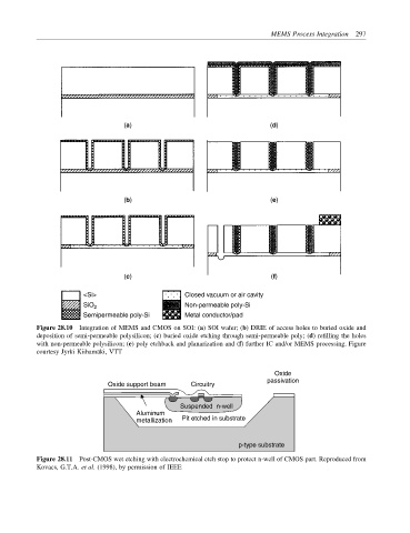
(a) (d)
(b) (e)
(c) (f)
<Si> Closed vacuum or air cavity
SiO 2 Non-permeable poly-Si
Semipermeable poly-Si Metal conductor/pad
Figure 28.10 Integration of MEMS and CMOS on SOI: (a) SOI wafer; (b) DRIE of access holes to buried oxide and
deposition of semi-permeable polysilicon; (c) buried oxide etching through semi-permeable poly; (d) refilling the holes
with non-permeable polysilicon; (e) poly etchback and planarization and (f) further IC and/or MEMS processing. Figure
courtesy Jyrki Kiiham¨ aki, VTT
Oxide
passivation
Oxide support beam Circuitry
Suspended n-well
Aluminum
metallization Pit etched in substrate
p-type substrate
Figure 28.11 Post-CMOS wet etching with electrochemical etch stop to protect n-well of CMOS part. Reproduced from
Kovacs, G.T.A. et al. (1998), by permission of IEEE