
Page 315 - Sami Franssila Introduction to Microfabrication
P. 315
294 Introduction to Microfabrication
Process flow for ink jet: (photoresist stripping and resistant to alkaline etchants). Through-wafer etching is
cleaning steps omitted) non-critical because it will stop automatically on the
bottom oxide of the flow tube.
thermal oxidation, 1 µm thick
lithography step 1: chip area definition
oxide etching 28.4 PATTERNING OVER SEVERE TOPOGRAPHY
boron diffusion, 2 µm deep
lithography step 2: chevron pattern: 1 µm width 28.4.1 Resist technology
RIE of silicon, 4 µm deep
anisotropic silicon etching to undercut p ++ chevrons Spray coating of resist works for wet-etched deep
structures with 54.7 angles but exposure focus depth
◦
thermal oxidation, 0.5 µm
is another issue. Electrochemical coating of resist is a
LPCVD nitride deposition for chevron roof sealing,
0.6 µm standard technique in the printed circuit board industry
etchback (or polishing) of nitride and negative working electrodeposited resist can cover
LPCVD polysilicon deposition, 0.8 µm sidewalls of vertical holes and cavities. However,
poly doping, 20 ohm/sq electrodeposited resist can be used for many ordinary
lithography step 3: poly-heater pattern applications as well. Even though its resolution is not
polysilicon etching stellar, it can be handy for large structures.
aluminium sputtering
lithography step 4: metal pads 28.4.2 Peeling masks/nested masks
aluminium etching
passivation: CVD oxide 1 µm + PECVD nitride 0.3 µm Photoresist coating over severe topography can be
lithography step 5: opening of bonding pads eliminated by double masking (peeling masks/nested
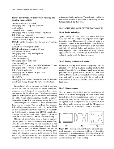
RIE of nitride and oxide masks, Figure 28.7): two different mask materials are
lithography step 6: pattern for gold lift-off patterned on a planar wafer, before the first deep
evaporation of Cr/Au etching. The first mask is discarded after the first etching
lift of Cr/Au step, and etching continues with the second mask.
lithography step 7: fluidic inlet definition on the backside Combinations of oxide, nitride and silicon carbide have
anisotropic etching through the wafer from the back. been tried.
Boron-doped silicon provides mechanical strength
for the structure, as compared to nitride membrane, 28.4.3 Shadow masks
which can be only hundreds of nanometres thick, versus
micrometres for the silicon roof. The chevron patterns Shadow masks (Figure 28.8) enable metallization of
open fast etching crystal planes that enable undercutting wafers with severe topography or even wafers with
on <100> wafer. Chevron openings must be as narrow through-holes. However, pattern size control over severe
as possible so that flow tube sealing is easy: however, topography may not be very good because of flux
0.5 µm oxide plus 0.6 µm nitride is much more than the divergence. It can be improved if the shadow mask itself
1 µm chevron opening. This has at least three reasons: is a silicon wafer patterned to match the 3D geometry
already fabricated, patterning accuracy is regained.
RIE etching results in some widening, thermal oxide is
ca. 50% inside silicon sidewalls and does not contribute
its full thickness to sealing; and LPCVD nitride step
coverage can be less than 100%. Figure 23.13 shows
what the chevrons look like before and after sealing.
Thinning of nitride/oxide stack is done to improve
thermal speed: the closer the heater resistor is to the flow
tube, the faster the heating will be. Aluminium is not
absolutely required because polysilicon is heavily doped (a) (b) (c)
and it can be used for wiring. However, aluminium Figure 28.7 Peeling mask/nested mask: (a) nitride (hat-
wiring reduces resistive losses. Gold on bonding pads ched) deposition and patterning; oxide (grey) deposition
makes wire bonding easy, and gold protects the front and patterning; first silicon etching; (b) oxide etching in HF;
side during backside anisotropic etching (areas that are second silicon etching with nitride mask and (c) capacitive
not gold-covered are either nitride or oxide, which are accelerometer by three-wafer bonding