
Page 313 - Sami Franssila Introduction to Microfabrication
P. 313
292 Introduction to Microfabrication
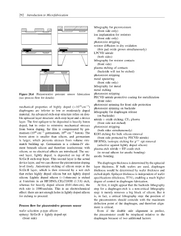
lithography for piezoresistors
(front side only)
ion implantation for resistors
(front side only)
photoresist stripping
resistor diffusion in dry oxidation
(thin pad oxide grown simultaneously)
LPCVD nitride
(both sides)
lithography for resistor contacts
(front side)
plasma etching of contacts
(backside will not be etched)
photoresist stripping
metal sputtering
(front side only)
lithography for metal
metal etching
Figure 28.4 Piezoresistive pressure sensor fabrication photoresist stripping
(see process flow for details) PECVD nitride protective coating for metallization
(front side)
photoresist spinning for front side protection
18
−3
mechanical properties of highly doped (>10 cm ) photoresist spinning on backside
diaphragms are inferior to low or moderately doped lithography for diaphragm release
material. An advanced etch-stop structure relies on dou- (on backside)
ble epitaxial layer structure: etch-stop layer and a device nitride + oxide etching; CF 4 plasma
layer. The first epilayer to be deposited is heavily boron (front side not etched)
doped, but in order to minimize mechanical stresses photoresist stripping
from boron doping, the film is compensated by ger- (both sides simultaneously)
20
21
manium (10 cm −3 germanium, 10 cm −3 boron). The KOH etching for bulk silicon removal
boron atom is smaller than silicon, and germanium (front side protected by PECVD nitride)
is larger, which prevents stresses from volume mis- HF:HNO 3 isotropic etching for p ++ epi removal
match building up. Germanium is a column-IV ele- (selective against lightly doped silicon)
ment beneath silicon and therefore isoelectronic with plasma-etch nitride + HF-oxide etch
silicon, so no electrical effects are introduced. The sec- (to reveal silicon for anodic bonding)
ond layer, lightly doped, is deposited on top of the anodic bonding.
Si:Ge:B etch-stop layer. This second layer is the actual
device layer, and we can choose the piezoresistor-doping The diaphragm thickness is determined by the epitaxial
level freely. Anisotropic etching of silicon stops at the layer thickness. If bulk wafers are used, diaphragm
Si:Ge:B layer, which is then removed by a wet etch thickness would be determined by wafer thickness and
that etches highly doped silicon but not lightly doped etched depth. Epilayer thickness is independent of wafer
silicon. Lightly doped silicon (>1 ohm-cm) is etched specifications (thickness, TTV), enabling a much higher
at 1 nm/min in an HF:HNO 3 :CH 3 COOH (1:3:8) etch, degree of control in diaphragm fabrication.
whereas for heavily doped silicon (0.01 ohm-cm), the At first, it might appear that the backside lithography
etch rate is 1000 nm/min. This is an electrochemical step for a diaphragm-etch is a non-critical lithography
effect: there are not enough holes in lightly doped silicon step: it merely removes a big block of silicon. But it
for etching to proceed. is, in fact, a critical lithography step: the position of
the piezoresistors should coincide with the maximum
deflection point of the diaphragm, and therefore align-
Process flow for piezoresistive pressure sensor
ment is critical.
wafer selection: p-type silicon Even if the double side alignment is perfect,
epitaxy: Si:Ge:B + lightly doped epi the piezoresistor could be misplaced relative to the
(front side) diaphragm because of two additional factors: