
Page 314 - Sami Franssila Introduction to Microfabrication
P. 314
MEMS Process Integration 293
1. If the wafer thickness is not exactly known, the top-side processes: lithography, oxide etching and boron
diaphragm size will be wrong (epitaxial layer does diffusion. This approach not only solves thickness and
not help here). Too thick a wafer will result in a TTV problems but also enables free-form nozzle shapes
diaphragm smaller than designed, and vice versa. to be fabricated, whereas simple anisotropic etching
Piezoresistors on the wafer front side will not results in square and rectangular nozzles only.
coincide with mis-sized diaphragm. Despite all the good features of anisotropic wet
2. If the etch selectivity between the (100) and (111) etching, through-wafer structures take up a lot of silicon
planes is not accurately known and included in the area. Nozzles fabricated by anisotropic through-wafer
mask design, the size of the diaphragm will be wrong. wet etching cannot be packed close to each other, and
for ink-jet printers, other nozzle geometries have been
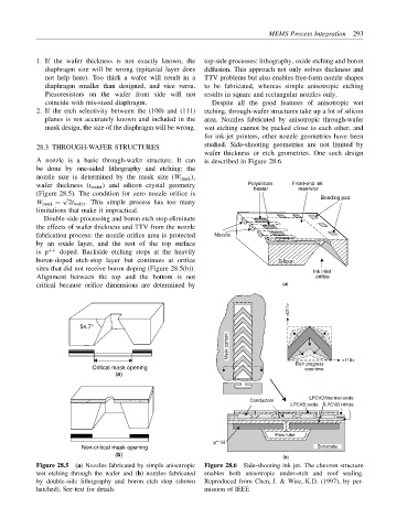
studied. Side-shooting geometries are not limited by
28.3 THROUGH-WAFER STRUCTURES
wafer thickness or etch geometries. One such design
A nozzle is a basic through-wafer structure. It can is described in Figure 28.6.
be done by one-sided lithography and etching: the
nozzle size is determined by the mask size (W mask ),
wafer thickness (t wafer ) and silicon crystal geometry Polysilicon Front-end ink
heater
reservoir
(Figure 28.5). The condition for zero nozzle orifice is
√ Bonding pad
W mask = 2t wafer . This simple process has too many
limitations that make it impractical.
Double-side processing and boron etch stop eliminate
the effects of wafer thickness and TTV from the nozzle
fabrication process: the nozzle orifice area is protected Nozzle
by an oxide layer, and the rest of the top surface
is p ++ doped. Backside etching stops at the heavily
boron-doped etch-stop layer but continues at orifice Silicon
sites that did not receive boron doping (Figure 28.5(b)).
Ink inlet
Alignment between the top and the bottom is not orifice
critical because orifice dimensions are determined by (a)
<011>
54.7°
Mask pattern
Etch progress <110>
Critical mask opening over time
(a)
LPCVD/thermal oxide
Conductors
LPCVD oxide LPCVD nitride
Flow tube
p ++ Si
Non-critical mask opening Substrate
(b) (b)
Figure 28.5 (a) Nozzles fabricated by simple anisotropic Figure 28.6 Side-shooting ink jet. The chevron structure
wet etching through the wafer and (b) nozzles fabricated enables both anisotropic under-etch and roof sealing.
by double-side lithography and boron etch stop (shown Reproduced from Chen, J. & Wise, K.D. (1997), by per-
hatched). See text for details mission of IEEE