
Page 312 - Sami Franssila Introduction to Microfabrication
P. 312
MEMS Process Integration 291
processing and materials can be selected from a device Shallow etches in the micron range are easy, and
operation point of view, and no extra protective coatings shallower ones could be made. However, the anodic
are needed during processing. bonding process and glass structural stability determine
how shallow passages shall remain open (as discussed
in Chapter 17). Auxiliary pillars (on the first mask) act
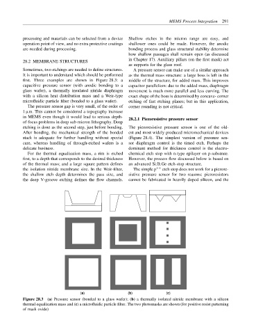
28.2 MEMBRANE STRUCTURES
as supports for the glass roof.
Sometimes, two etchings are needed to define structures. A pressure sensor can make use of a similar approach
It is important to understand which should be performed as the thermal mass structure: a large boss is left in the
first. Three examples are shown in Figure 28.3: a middle of the structure, for added mass. This improves
capacitive pressure sensor (with anodic bonding to a capacitor parallelism: due to the added mass, diaphragm
glass wafer), a thermally insulated nitride diaphragm movement is much more parallel and less curving. The
with a silicon heat distribution mass and a Weir-type exact shape of the boss is determined by concave- corner
microfluidic particle filter (bonded to a glass wafer). etching of fast etching planes; but in this application,
The pressure sensor gap is very small, of the order of corner rounding is not critical.
1 µm. This cannot be considered a topography increase
in MEMS even though it would lead to serious depth-
28.2.1 Piezoresistive pressure sensor
of-focus problems in deep sub-micron lithography. Deep
etching is done as the second step, just before bonding. The piezoresistive pressure sensor is one of the old-
After bonding, the mechanical strength of the bonded est and most widely produced micromechanical devices
stack is adequate for further handling without special (Figure 28.4). The simplest version of pressure sen-
care, whereas handling of through-etched wafers is a sor diaphragm control is the timed etch. Perhaps the
delicate business. dominant method for thickness control is the electro-
For the thermal equalization mass, a rim is etched chemical etch stop with n-type epilayer on p-substrate.
first, to a depth that corresponds to the desired thickness However, the process flow discussed below is based on
of the thermal mass; and a large square pattern defines an advanced Si:B:Ge etch-stop structure.
the isolation nitride membrane size. In the Weir-filter, The simple p ++ etch stop does not work for a piezore-
the shallow etch depth determines the pass size, and sistive pressure sensor for two reasons: piezoresistors
the deep V-groove etching defines the flow channels. cannot be fabricated in heavily doped silicon, and the
(a) (b) (c)
Figure 28.3 (a) Pressure sensor (bonded to a glass wafer); (b) a thermally isolated nitride membrane with a silicon
thermal equalization mass and (c) a microfluidic particle filter. The two photomasks are shown (for positive resist patterning
of mask oxide)