
Page 310 - Sami Franssila Introduction to Microfabrication
P. 310
MEMS Process Integration 289
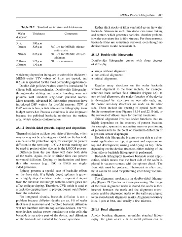
Table 28.2 Standard wafer sizes and thicknesses Rather thick stacks of films can build up on the wafer
backside. Stresses in such film stacks can cause flaking
Wafer Thickness Comments and rupture, which generates particles. Another problem
diameter
is wafer curvature due to film stresses. For these reasons,
backside films are sometimes removed even though no
3 in. 380 µm
100 mm 525 µm 380 µm for MEMS; thinner device reason would necessitate it.
wafers exist
150 mm 625 µm 380 µm for MEMS; 250 µm 28.1.3 Double-side lithography
minimum
200 mm 725 µm 500 µm minimum Double-side lithography comes with three degrees
300 mm 770 µm of difficulty:
• arrays without alignment;
which may depend on the square or cube of the thickness). • non-critical alignment;
MEMS-wafer TTV values of 1 µm are typical, and • critical alignment.
0.5 µm is specified for the most demanding applications.
Double-side polished wafers were first introduced for Regular array structures on the wafer backside
silicon bulk micromechanics. Double-side lithography, without alignment to the front include, for example,
through-wafer etching and anodic bonding were not solar-cell back surface field diffusion (Figure 1.6). In
possible with standard single-side polished wafers. non-critical alignment, the major function of the device
More recently, advanced IC fabrication processes have is determined by structures on one side only, and
introduced DSP wafers for twofold reasons: TTV of the coarse auxiliary structures are made on the other
DSP wafers is less, which relieves the lithography focus side. These include the opening of optical paths and
budget somewhat. Process cleanliness is also improved fluidic connections (see Figures 11.14 and 22.11(a)), or
because the polished backside minimizes the surface the removal of silicon mass for thermal insulation.
area, which reduces contamination. Critical alignment involves device functions that are
highly dependent on the accuracy of pattern location,
for example, symmetric resonating mass or positioning
28.1.2 Double-sided growth, doping and deposition
of piezoresistors to the point of maximum deflection of
Thermal oxidation oxidizes both sides of the wafer, which a pressure sensor diaphragm.
may or may not be advantageous. Oxide on the backside Double-side lithography is done on one side at a time:
can be a useful protective layer, for example, to prevent resist application on top, alignment and exposure on
diffusion in the next step. LPCVD nitride masking can top and development, rinsing and drying on top. Then,
be used to protect either side, as in the LOCOS process. depending on the device structure, either etching of the
Diffusion from the gas phase will dope both sides front-side or backside lithography is performed.
of the wafer. Again, oxide or nitride films can prevent Backside lithography involves backside resist appli-
unwanted diffusion. Doping by implantation and from cation, which means that the front side of the wafer is
thin film sources (e.g., PSG or BSG) are single- placed in vacuum contact with the spinner chuck. The
sided processes. front side must be protected. Photoresist is often used
Epitaxy presents a special case of backside effects but it cannot be used for patterning after being vacuum-
on the front side: if a lightly doped epilayer is grown chucked.
on a highly doped substrate wafer, evaporated dopant The alignment mechanism in double-sided lithogra-
from the substrate will mingle with the source gases and phy (Figure 28.2) relies on image processing. The image
affect epilayer doping. Therefore, CVD oxide is used as of the mask alignment marks is stored, the wafer is then
a backside-capping layer to prevent dopant outdiffusion inserted between the mask and the alignment micro-
from the substrate. scope, and the alignment marks on the wafer are aligned
For integrated circuits, backside diffusion is not a to the stored mask alignment marks. Alignment accuracy
problem because diffusion depths are ca. 1% of wafer is ca. 1 µm at best, and usually a few microns.
thickness at maximum and therefore backside diffusions
will not interfere with the top surface devices. For vol- 28.1.4 Bond alignment
ume devices such as power transistors or solar cells, the
backside is an active part of the device, and diffusions Anodic bonding alignment resembles standard lithog-
on the backside are essential for device operation. raphy: the glass wafer with its metal patterns can be