
Page 305 - Sami Franssila Introduction to Microfabrication
P. 305
284 Introduction to Microfabrication
(a) (b) (c) (d)
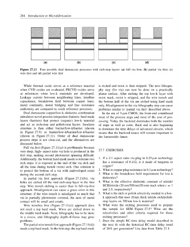
Figure 27.11 Four possible dual damascene processes with etch-stop layers: (a) full via first; (b) partial via first; (c)
wire first and (d) partial wire first
While thermal oxide serves as a reference material is etched and resist is then stripped. The next lithogra-
when CVD oxides are evaluated, PECVD oxides serve phy step (for via) can now be done on a practically
as references when low-k materials are developed. planar surface. After etching the top low-k layer with
Leakage current between neighboring lines, interline resist mask, resist is stripped, and the wire trench and
capacitance, breakdown field between copper lines, the bottom half of the via are etched using hard mask
metal continuity, metal bridging and line resistance only. Misalignment in the via-lithography step can cause
uniformity are compared to oxide reference processes. problems similar to ‘partial via first’ described above.
Dual damascene copper/low-k dielectric combination In the era of 5 µm CMOS, the front-end contributed
introduces novel process integration features: hard mask most of the process steps and most of the cost of pro-
layers (barriers) that protect (organic) low-k material cessing. Today the backend dominates both the number
and act as etch-stop and polish-stop layers. Insulator of steps as well as costs. Back end is also beginning
structure is then either barrier/low-k/barrier (shown to dominate the time delays of advanced circuits, which
in Figure 27.9) or barrier/low-k/barrier/low-k/barrier means that the backend issues will remain important in
(shown in Figure 27.11). Order of dual damascene the foreseeable future.
process steps is not clear-cut, and the alternatives are
discussed below.
Full via first (Figure 27.11(a)) is problematic because
very deep, high- aspect ratio via hole is produced in the 27.7 EXERCISES
first step, making second photoresist spinning difficult.
Additionally, the bottom hard mask needs to tolerate two 1. If a 2:1 aspect ratio via plug in 0.25 µm technology
etch steps: it is exposed in the end of the via etch and has a resistance of 0.4 , is it made of tungsten or
all the time during trench (wire) etch. One solution is copper?
to protect the bottom of a via with undeveloped resist 2. What is copper plug resistance in 0.1 µm technology?
during the second etch step. 3. What is the breakdown field requirement for low-k
In partial via first approach (Figure 27.11(b)), via dielectrics?
holes are etched till the mid etch-stop layer in the first 4. What is the effective dielectric constant of nitride/
step. Wire trench etching is easier than in full-via-first BCB/nitride (20 nm/500 nm/20 nm) stack when ε = 7
approach. Misalignment can cause a grave error in this and 2.5, respectively?
structure: if the wire trench is misaligned so much that 5. What is the etch or polish selectivity needed in a low-
via is partially photoresist covered, the area of metal k approach that uses 20 nm thick nitride etch/polish-
contact will be small and erratic. stop layers on 300 nm low-k material?
Wire trenches first (Figure 27.11(c)) approach does 6. What were the etching processes used to prepare
not need a top hard mask. Wires are etched down to the sample for SEM Figure 27.5? What are the
the middle hard mask. Next, lithography has to be done selectivities and other criteria required for those
in a recess, and lithography depth-of-focus may pose etching processes?
problems. 7. Does the simple RC-time delay model described in
The partial wire trench first approach (Figure 27.11(d)) the next fit with the historical RC-time delay trend
needs a top hard mask. In the first step, the top hard mask of 26% per generation? Use data from Table 27.1.