
Page 302 - Sami Franssila Introduction to Microfabrication
P. 302
Multilevel Metallization 281
W Table 27.1 Backend scaling trends
CMOS 0.35 µm 0.25 µm 0.18 µm 0.13 µm
generation
T
L Min. metal 0.4 0.3 0.22 0.15
H
Metal linewidth/µm
Min. space/µm 0.6 0.45 0.33 0.25
Dielectric Metal 0.7 0.6 0.4 0.4
thickness/µm
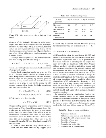
Figure 27.8 Wire geometry for simple RC-time delay Dielectric 1 0.84 0.70 0.6
model thickness/µm
direction. If the dielectric thickness is scaled down,
1.8 µohm-cm) and silicon dioxide dielectrics (ε ≈ 4)
capacitance between metal layers increases, leading to
have been replaced by low-k dielectrics (1 < ε < 4).
increased RC-time delays. At 1 µm linewidths, transistor
delays are more significant than wiring delays, but the
situation changes somewhere around 0.2 µm technology, 27.5 COPPER METALLIZATION
and below 100 nm wiring delay clearly dominates over
transistor delays. All ICs used aluminium for metallization till 1997, and
A simple model (Figure 27.8) for backend intercon- most still do, but copper has been introduced into high-
nect wire scaling gives RC-time delay as performance applications from 0.25 µm generation on.
Resistance reduction is advantageous but copper has
τ = RCL 2 C = εWL/T R = ρL/HW many drawbacks and limitations (Table 27.2). Copper
(27.1) diffuses rapidly in both silicon and silicon oxides, and
where L is line length and resistance R and capacitance new barrier materials have to be invented: tantalum and
C are per unit length. its compounds and alloys are prime candidates. Copper
Scaled local connection lengths are given by L/n has to be chemical–mechanical polished, so CMP is
(n > 1) because smaller devices are closer to each a must. Whereas aluminium deposition is always by
other. Long distance connections do not scale, however, sputtering and tungsten is by CVD, there are a number
because chips are not getting any smaller, quite the of copper deposition methods available: electroless,
contrary, in fact, because more and more functions are electroplating, CVD and sputtering. Sputtering is ruled
crammed on a chip. In our simple model, we will out because of poor step coverage and inability to fill
assume a constant line length, L. Scaled capacitance holes, but it can still be used to deposit a thin seed layer
and resistance are given by for electrodeposition. Both CVD and electrodeposition
methods can fill high-aspect ratios encountered in deep
′
C = ε(W/n)L/(T /n) = C (27.2)
submicron devices.
2
′
R = ρL/(H/n)(W/n) = n R (27.3) In aluminium/tungsten metallization, barriers are
needed between metals but in copper metallization
RC-time delay τ is then given by barriers are required for dielectrics as well (it is of course
′
possible to develop new dielectric materials that would
2
′
′
′
τ = R C = n RC (27.4)
be stable in contact with copper, but currently copper
needs to be clad from all four sides, see Figure 27.9).
Because scaling factor n is larger than unity, time delays
are increasing. When linewidths are scaled down, film
thicknesses are scaled down in order to keep aspect Table 27.2 Issues in copper metallization
ratios about the same (Table 27.1), which is not an
unreasonable assumption since very tall but narrow – Adhesion to dielectric
metal lines would be difficult to make. Because chip – Diffusion in (and reaction with) dielectric
sizes (L) are increasing, time delays are bound to – – Compatibility with tungsten contact plug
Deposition of seed layer
increase. Historically, RC-time delay has increased 26% – Deposition of copper
per generation.
– Contamination on the chip
In order to battle RC-time delay, aluminium (ρ ≈
– Contamination in the equipment
3 µohm-cm) has been replaced by copper (ρ ≈