
Page 298 - Sami Franssila Introduction to Microfabrication
P. 298
27
Multilevel Metallization
Multiple levels of metallization offer possibilities for emerged in the late 1990s, and more recently low dielec-
circuit designers to route signals over transistors, and tric constant materials (low-k) have been introduced.
thus to reduce the area needed for wiring. Multi- These are completely new materials, driven by CMOS-
level metallization structures for submicron technolo- metallization time delay concerns.
gies (0.8/0.5/0.35/0.25 µm) are based on aluminium
with two process technology innovations: contact and
via filling with plugs of tungsten CVD and oxide pla- 27.1 TWO-LEVEL METALLIZATION
narization by CMP (Figure 27.1). Copper metallization
Two-level metallizations are extensions of one-level
metallizations (see Figure 25.2(i)), with additional di-
electric and metal films and only minor conceptual
differences. The process continues after first metal as
follows:
M5
V4 Process flow for two-level metallization
M4
intermetal dielectric PECVD oxide
V3 planarization SOG etchback
via holes oxide plasma etch
M3 second metal deposition TiW/Al sputtering
metal etching Cl 2 -based plasma
V2
passivation PECVD nitride
bonding pad open CF 4 -plasma etch
M2
V1 There are a number of practical aspects in two-level
metal processes that demand attention. Each additional
M1
(PE)CVD step adds to thermal loads, causes stresses
CA and plasma damage. Silicon/metal interface stability
M0 needs to be rechecked and barrier re-evaluated. Stresses
from additional layers can cause hillock growth and
crack propagation, which must be checked. Hillock
PC
sizes are amenable to optical microscope inspection,
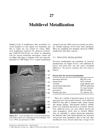
Figure 27.1 Cross-sectional view of six level metal struc- but electrical data from short/continuity test structures
tures (M0 is metal zero). Reproduced from Koburger, C.W. will provide more quantitative data on this and other
et al. (1995), by permission of IBM metallization issues. Second metal step coverage in the
Introduction to Microfabrication Sami Franssila
2004 John Wiley & Sons, Ltd ISBNs: 0-470-85105-8 (HB); 0-470-85106-6 (PB)