
Page 294 - Sami Franssila Introduction to Microfabrication
P. 294
Bipolar Technology 273
B
B
Nitride
SiO 2 + p + SiO 2
p ++ n p ++ p ++ p p p ++
n
(a) (c)
B
+
Nitride n −Poly SiO
SiO 2 ++ p + p + ++ 2
+
+
p ++ p n p p ++ p n p
n + p
(b) (d)
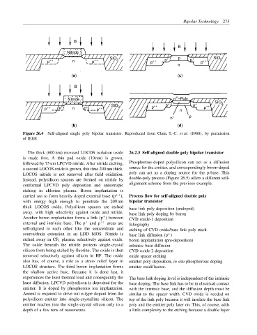
Figure 26.4 Self-aligned single poly bipolar transistor. Reproduced from Chen, T.-C. et al. (1988), by permission
of IEEE
The thick (600 nm) recessed LOCOS isolation oxide 26.2.3 Self-aligned double poly bipolar transistor
is made first. A thin pad oxide (10 nm) is grown,
followed by 75 nm LPCVD nitride. After nitride etching, Phosphorous-doped polysilicon can act as a diffusion
a second LOCOS oxide is grown, this time 200 nm thick. source for the emitter, and correspondingly boron-doped
LOCOS nitride is not removed after field oxidation. poly can act as a doping source for the p-base. This
double-poly process (Figure 26.5) offers a different self-
Instead, polysilicon spacers are formed on nitride by
alignment scheme from the previous example.
conformal LPCVD poly deposition and anisotropic
etching in chlorine plasma. Boron implantation is
carried out to form heavily doped external base (p ++ ), Process flow for self-aligned double poly
with energy high enough to penetrate the 200 nm bipolar transistor
thick LOCOS oxide. Polysilicon spacers are etched base link poly deposition (undoped)
away, with high selectivity against oxide and nitride. base link poly doping by boron
+
Another boron implantation forms a link (p ) between CVD oxide-1 deposition
external and intrinsic base. The p + and p ++ areas are lithography
self-aligned to each other like the source/drain and etching of CVD oxide/base link poly stack
source/drain extension in an LDD MOS. Nitride is base link diffusion (p )
+
etched away in CF 4 plasma, selectively against oxide. boron implantation (pre-deposition)
The oxide beneath the nitride protects single-crystal intrinsic base diffusion
silicon from being etched by fluorine. The oxide is then CVD oxide-2 deposition
removed selectively against silicon in HF. The oxide oxide spacer etching
also has, of course, a role as a stress relief layer in emitter poly deposition, in situ phosphorous doping
LOCOS structure. The third boron implantation forms emitter outdiffusion.
the shallow active base. Because it is done last, it
experiences the least thermal load and consequently the The base link doping level is independent of the intrinsic
least diffusion. LPCVD polysilicon is deposited for the base doping. The base link has to be in electrical contact
emitter. It is doped by phosphorous ion implantation. with the intrinsic base, and the diffusion depth must be
Anneal is required to drive out n-type dopant from the similar to the spacer width. CVD oxide is needed on
polysilicon emitter into single-crystalline silicon. The top of the link poly because it will insulate the base link
emitter reaches into the single-crystal silicon only to a poly and the emitter poly later on. This, of course, adds
depth of a few tens of nanometres. a little complexity to the etching because a double layer