
Page 291 - Sami Franssila Introduction to Microfabrication
P. 291
270 Introduction to Microfabrication
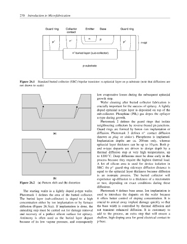
Guard ring Collector Emitter Base Guard ring
contact
n p
p + n + p + n-epi
+
n buried layer (sub-collector)
p-substrate
Figure 26.1 Standard buried collector (SBC) bipolar transistor: n-epitaxial layer on p-substrate (note that diffusions are
not drawn to scale)
low evaporative losses during the subsequent epitaxial
growth step.
Wafer cleaning after buried collector fabrication is
crucially important for the success of epitaxy. A lightly
doped epitaxial n-type layer is deposited on top of the
sub-collector. Phosphine (PH 3 ) gas dopes the epilayer
n-type during growth.
Photomask 2 defines the guard rings that isolate
neighbouring collectors by reverse-biased pn-junctions.
Guard rings are formed by boron–ion implantation or
(a) diffusion. Photomask 3 defines n + contact diffusion
(known as plug or sinker). Phosphorus is implanted.
Implantation depths are ca. 200 nm only, whereas
epitaxial layer thickness can be up to 10 µm. Both p-
and n-type dopants are driven to design depth by a
thermal diffusion step at very high temperatures, up
◦
to 1200 C. Deep diffusions must be done early in the
process because they require the highest thermal load.
A lot of silicon area is used for device isolation in
SBC: the p guard ring sideways diffusion distance is
+
equal to the epitaxial layer thickness because diffusion
is an isotropic process. The buried collector will
(b) experience up-diffusion to a thickness of a micrometre
Figure 26.2 (a) Pattern shift and (b) distortion or two, depending on exact conditions during these
diffusions.
The starting wafer is a lightly doped p-type wafer. Photomask 4 defines base areas. Ion implantation is
Photomask 1 defines the area of the buried collector. used to introduce the dopants on the wafer because
The buried layer (sub-collector) is doped to a high it offers better control of doping concentration. It is
concentration either by ion implantation or by furnace crucial to anneal away implant damage quickly so that
diffusion (Figure 26.3(a)). If implantation is done, the the base width is controlled by thermal diffusion and
annealing step must be carried out for damage removal not transient enhanced diffusion. It is customary to
and recovery of a perfect silicon surface for epitaxy. add to the process, an extra step that will ensure a
Antimony is often used as the buried layer dopant shallow, high-doping area for good electrical contact to
because of its low vapour pressure, and consequently p-base.