
Page 287 - Sami Franssila Introduction to Microfabrication
P. 287
266 Introduction to Microfabrication
plasma etching, but re-grown during poly oxidation.
Calculate the oxide thickness under the following
assumptions:
• poly etch rate is 250 nm/min;
• poly thickness is 250 nm;
• Si:SiO 2 etch selectivity is 20:1;
• overetch time is 20 s;
• re-oxidation is 900 C, 10 min (dry).
◦
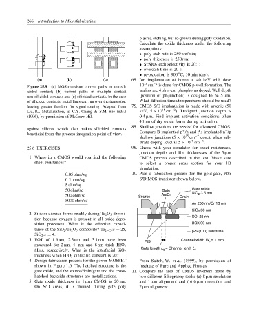
(a) (b) (c) 6S. Ion implantation of boron at 40 keV with dose
13
Figure 25.9 (a) MOS-transistor current paths in non-sil- 10 cm −2 is done for CMOS p-well formation. The
icided contact; (b) current paths in multiple contact wafers are 4 ohm-cm phosphorus doped. Well depth
non-silicided contacts and (c) silicided contacts. In the case (position of pn-junction) is designed to be 5 µm.
of silicided contacts, metal lines can run over the transistor, What diffusion times/temperatures should be used?
leaving greater freedom for signal routing. Adapted from 7S. CMOS S/D implantation is made with arsenic (50
15
−2
Liu, R., Metallization, in C.Y. Chang & S.M. Sze (eds.) keV, 5 × 10 cm ). Designed junction depth is
(1996), by permission of McGraw-Hill 0.4 µm. Find implant activation conditions when
40 nm of dry oxide forms during activation.
8S. Shallow junctions are needed for advanced CMOS.
against silicon, which also makes silicided contacts + +
beneficial from the process integration point of view. Compare B-implanted p /n and As-implanted n /p
−2
15
shallow junctions (5 × 10 cm dose), when sub-
−3
17
strate doping level is 5 × 10 cm .
25.6 EXERCISES 9S. Check with your simulator for sheet resistances,
junction depths and film thicknesses of the 5 µm
1. Where in a CMOS would you find the following CMOS process described in the text. Make sure
sheet resistances? to select a proper cross section for your 1D
simulation.
0.05 ohm/sq 10. Plan a fabrication process for the gold-gate, PtSi
0.5 ohm/sq S/D MOS-transistor shown below.
5 ohm/sq
50 ohm/sq Gate Gate oxide
500 ohm/sq Source Au/Cr Drain SiO 2 3.5 nm
5000 ohm/sq
Au 250 nm/Cr 10 nm
SiO 2 80 nm
2. Silicon dioxide forms readily during Ta 2 O 5 deposi-
SOI 25 nm
tion because oxygen is present in all oxide depo-
sition processes. What is the effective capaci- BOX 90 nm
tance of the SiO 2 /Ta 2 O 5 composite? Ta 2 O 5 :ε = 25,
p-Si(100) substrate
SiO 2 :ε = 4.
3. EOT of 1.9 nm, 2.3 nm and 3.1 nm have been Channel width W c = 1 mm
PtSi
measured for 2 nm, 4 nm and 8 nm thick HfO 2
Gate length L g = Channel lenth L c
films, respectively. What is the interfacial SiO 2
thickness when HfO 2 dielectric constant is 20?
4. Design fabrication process for the power-MOSFET From Saitoh, W. et al. (1999), by permission of
shown in Figure 1.6. The hatched structure is the Institute of Pure and Applied Physics.
gate oxide, and the source/drain/gate and the cross- 11. Compare the area of CMOS inverters made by
hatched backside structures are metallizations. two different lithography tools: (a) 8 µm resolution
5. Gate oxide thickness in 1 µm CMOS is 20 nm. and 1 µm alignment and (b) 6 µm resolution and
On S/D areas, it is thinned during gate poly 2 µm alignment.