
Page 284 - Sami Franssila Introduction to Microfabrication
P. 284
CMOS Transistor Fabrication 263
thicknesses are scaled down. Metals and organics can Equivalent oxide thickness, EOT, is often used in
be removed from the wafers by cleaning, but for very describing high-ε dielectrics that replace silicon dioxide.
thin oxides, impurities in the gas phase also matter: Equivalent oxide thickness is given by
residual water vapour at 20 ppm concentration level
in the oxidation tube will dramatically enhance dry EOT = (ε SiO 2 /ε high ) × t high−ε + t SiO 2 (25.6)
oxidation rate. Surface roughness also affects oxide is the interfacial silicon dioxide thickness,
where t SiO 2
electrical quality and channel mobility because in the if any.
MOS transistor, the current is confined to ca. 10 nm Zirconium oxide (ZrO 2 , ε ≈ 23) film of 6 nm thick-
silicon layer underneath the gate oxide. ness has EOT ≈1 nm, under the assumption of no inter-
Silicon dioxide has a lower thickness limit of ca. 2 nm facial SiO 2 . Even a 1 nm SiO 2 layer will cause a drastic
as a CMOS gate oxide because of leakage currents. effect on EOT. Furthermore, dielectric constants of very
One problem with ultra-thin gate oxides is boron thin films are different from bulk values or from values
+
penetration: boron from the p polysilicon can diffuse measured for thicker films (recall Figure 5.1). Note that
through the gate oxide into the channel during thermal we have used the classical capacitance formula above: in
treatments and change channel doping, and therefore the 3 nm thickness range, a quantum mechanical descrip-
threshold voltage. tion should be used for accurate results.
A number of methods and materials have been inves-
tigated as replacements for thermal oxide. Nitrided oxide 25.4.2 Self-aligned gate
(NO) and oxidation of nitrided oxide (ONO) are evolu-
tionary developments based on thermal oxidation. New The gate pattern is, together with contact holes, the
alternatives are deposited films, and this is a paradigm most demanding lithographic and etching challenge
of modern ICs. Gate linewidth scaling is a combined
shift. Table 25.8 is also a chronological sequence of
lithography and etching problem: feature size in the
developments: amorphous and polycrystalline deposited
resist versus etched feature size. Etching is also related
oxides are expected to be the next materials to be imple-
to gate oxide thickness: poly-gate etching has to stop on
mented; and single-crystal oxides and very high-k mate-
the thin gate oxide. The length of a gate level conductor
rials are still further in the future.
is only a few microns, or tens of microns, and low
Silicon dioxide is amorphous, and it stays amorphous
resistivity is not a major requirement. Instead, ease of
through the high-temperature steps; single-crystal oxides
would also be stable, but most amorphous oxides will patterning and thermal stability in the contact with the
crystallize and polycrystalline oxides will exhibit grain oxide are primary concerns.
growth, both of which lead to problems. Front-end The self-aligned polygate was a major milestone in
temperatures may have to be limited because of oxides, MOS evolution: source/drain diffusions were automati-
and not because of junction diffusion. cally aligned to the gate. But as transistor scaling con-
If, during deposition of the high dielectric–constant tinued, more complex doping patterns were called for.
material, silicon dioxide is formed at the interface, the One motivation was to reduce hot electron effects: high
system that is formed is a SiO 2 /high-ε two-layer struc- electric fields in the channel accelerate electrons to high
ture, which must be analysed as capacitors in series. energies, and these electrons can degrade the gate oxide.
Interfacial silicon dioxide formation is difficult to avoid In order to reduce these high electric fields, lightly doped
because high-ε dielectrics are oxides, and oxygen is drain (LDD) structure was introduced (Figure 25.6). In
present in some form or another during their deposition. LDD, source/drain implantation is done in two steps.
After polygate etching, a self-aligned, low-energy,
13
−2
low-dose (ca. 10 cm ) implant is done, followed
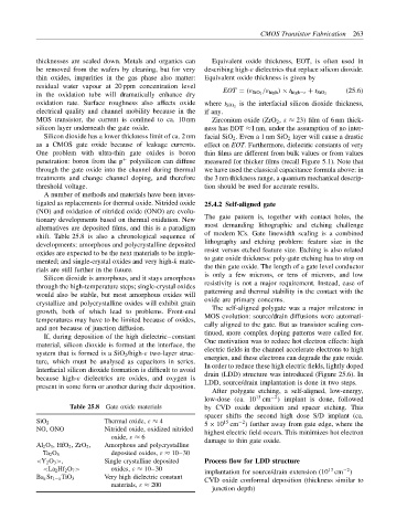
Table 25.8 Gate oxide materials by CVD oxide deposition and spacer etching. This
spacer shifts the second high dose S/D implant (ca.
−2
15
SiO 2 Thermal oxide, ε ≈ 4 5 × 10 cm ) further away from gate edge, where the
NO, ONO Nitrided oxide, oxidized nitrided
highest electric field occurs. This minimizes hot electron
oxide, ε ≈ 6
Al 2 O 3 , HfO 2 , ZrO 2 , Amorphous and polycrystalline damage to thin gate oxide.
Ta 2 O 5 deposited oxides, ε ≈ 10–30
<Y 2 O 3 >, Single crystalline deposited Process flow for LDD structure
<La 2 Hf 2 O 7 > oxides, ε ≈ 10–30 implantation for source/drain extension (10 cm )
13
−2
Ba x Sr 1−x TiO 3 Very high dielectric constant CVD oxide conformal deposition (thickness similar to
materials, ε ≈ 200
junction depth)