
Page 280 - Sami Franssila Introduction to Microfabrication
P. 280
CMOS Transistor Fabrication 259
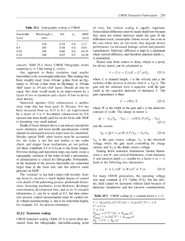
Table 25.2 Lithographic scaling of CMOS of view, but vertical scaling is equally important.
Source/drain diffusions must be made shallower because
Linewidth Wavelength λ NA k 1 DOF they must not extend sideways under the gate. If the
(µm) (nm) (µm)
diffusions touch, catastrophic failure occurs, but even in
the case where they do not touch, they degrade device
1 436 0.38 0.8 ±1.5
0.5 365 0.48 0.6 ±0.8 performance via increased leakage current and parasitic
0.25 248 0.60 0.6 ±0.35 capacitances. Sideways diffusion is kept to a minimum
0.18 248 0.65 0.5 ±0.30 when vertical diffusion, and therefore junction depth x j ,
is minimized.
Transit time from source to drain, which is a proxy
concern. Table 25.2 shows CMOS lithography trends for device speed, can be calculated as
assuming k 2 = 1 but letting k 1 evolve.
2
One approach to better resolution (and smaller τ = L/v = L/µE = L /µV ds (25.1)
linewidths) is by wavelength reduction. This strategy has
been steadily used: from 436 nm (g-line from an Hg- where L is channel length, v is the velocity and µ the
lamp) to 365 nm (i-line from an Hg-lamp) to 248 nm mobility of the electron in electric field E = V ds /L. The
(KrF laser) to 193 nm (ArF laser). Should all else be gate and the substrate form a capacitor, with the gate
equal, this alone would result in an improvement by a oxide as the capacitor dielectric of thickness T . The
factor of two in resolution and a factor of four in device gate capacitance is then
areal density.
Numerical aperture (NA) enhancement is another C = εWL/T (25.2)
clear route that has been used. In 20 years, NA has where W is the width of the gate and ε is the dielectric
been increased from ca. 0.15 to 0.7, an improvement constant of oxide. The charge in transit is
by a factor of 4 or 5. Resolution enhancement by NA
increase has been dearly paid for on the focus side: DOF Q = −C g (V gs − V th ) = −(εWL/T )(V gs − V th )
is becoming very small indeed (25.3)
Depth of focus defined above is an optical concept but and the current
resist chemistry and resist profile specifications (which
depend on subsequent process steps) must be considered. I ds = Q/τ = µεW/LT (V gs − V th )V ds (25.4)
Besides optical DOF, other factors must be accounted
for: the wafer is not flat and neither is the wafer V gs is the gate–source voltage, V th is the threshold
chuck, and stepper focus mechanisms are not perfect. voltage where the gate starts controlling the charge
All these contribute 0.1 to 0.2 µm to the focus budget. carriers and V ds is the drain–source voltage.
Previous etching and deposition steps can easily create a Scaling down transistor dimensions (lateral dimen-
topography variation of the order of half a micrometre, sions L and W, and vertical dimensions, oxide thickness
so planarization is critical for lithography. Fortunately, T and junction depth x j ), smaller by a factor n (n > 1)
in the backend of the process linewidths are somewhat leads to the following new dimensions:
larger than in the front end, and this relieves some ′ ′ ′
pressure on DOF. L = L/nW = W/nT = T /n (25.5)
The ‘constant’ k 1 has had a major role recently. Scal- For many CMOS generations, the operating voltage
ing down k 1 involves a much higher degree of control was kept constant at 5 V (Table 25.4), but the elec-
over details of the patterning process: photomask dimen- tric field cannot be increased without limit because of
sions, focussing mechanics, resist thickness, developer dielectric breakdown and hot electron considerations,
concentration, development time, and so on. In research
laboratories, k 1 can be as small as 0.3, but then exten-
sive process control measurements must be carried out. Table 25.3 CMOS scaling by a constant factor n (>1)
In volume manufacturing, k 1 has to be somewhat higher, τ = (1/µ)((L/n) /(V/n)) = (1/µ)(L /V ) = τ/n
2
2
′
for example, 0.5, for process robustness. ′
C = C/n
′
I = I/n
′2
′
′
′
25.2.2 Transistor scaling P switch = C V /2τ = P switch /n 2
E switch = (1/2)C V ′2 = E switch /n 3
′
′
CMOS transistor scaling (Table 25.3) is most often dis- P ′ = I V = P dc /n 2
′
′
cussed from the lithographic, linewidth-scaling point dc