
Page 278 - Sami Franssila Introduction to Microfabrication
P. 278
CMOS Transistor Fabrication 257
Resist Pad
Nitride oxide
n-substrate
NMOS PMOS
(a) (b)
Unmasked implant
Boron implant Arsenic implants Arsenic field stop
(c) (d)
(e) (f)
(g) (h)
(i)
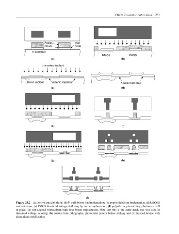
Figure 25.2 (a) Active area definition; (b) P-well: boron-ion implantation; (c) arsenic field stop implantation; (d) LOCOS
wet oxidation; (e) PMOS threshold voltage–tailoring by boron implantation; (f) polysilicon gate etching, photoresist still
in place; (g) self-aligned source/drain high-dose boron implantation. Note that this is the same mask that was used in
threshold voltage tailoring; (h) contact hole lithography, photoresist pattern before etching and (i) finished device with
aluminium metallization