
Page 297 - Sami Franssila Introduction to Microfabrication
P. 297
276 Introduction to Microfabrication
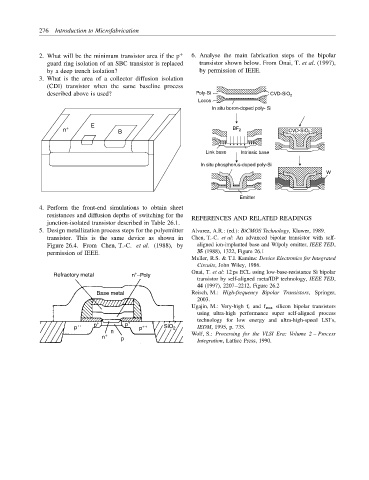
2. What will be the minimum transistor area if the p + 6. Analyse the main fabrication steps of the bipolar
guard ring isolation of an SBC transistor is replaced transistor shown below. From Onai, T. et al. (1997),
by a deep trench isolation? by permission of IEEE.
3. What is the area of a collector diffusion isolation
(CDI) transistor when the same baseline process
described above is used? Poly-Si CVD-SiO 2
Locos
In situ boron-doped poly- Si
E
n + B BF 2 CVD-SiO 2
Link base Intrinsic base
In situ phosphorus-doped poly-Si
W
Emitter
4. Perform the front-end simulations to obtain sheet
resistances and diffusion depths of switching for the REFERENCES AND RELATED READINGS
junction-isolated transistor described in Table 26.1.
5. Design metallization process steps for the polyemitter Alvarez, A.R.: (ed.): BiCMOS Technology, Kluwer, 1989.
transistor. This is the same device as shown in Chen, T.-C. et al: An advanced bipolar transistor with self-
Figure 26.4. From Chen, T.-C. et al. (1988), by aligned ion-implanted base and W/poly emitter, IEEE TED,
permission of IEEE. 35 (1988), 1322, Figure 26.1
Muller, R.S. & T.I. Kamins: Device Electronics for Integrated
Circuits, John Wiley, 1986.
Refractory metal n −Poly Onai, T. et al: 12 ps ECL using low-base-resistance Si bipolar
+
transistor by self-aligned meta/IDP technology, IEEE TED,
44 (1997), 2207–2212, Figure 26.2
Base metal Reisch, M.: High-frequency Bipolar Transistors, Springer,
2003.
Ugajin, M.: Very-high f t and f max silicon bipolar transistors
using ultra-high performance super self-aligned process
technology for low energy and ultra-high-speed LSI’s,
+
+
p ++ p p p ++ SiO 2 IEDM, 1995, p. 735.
n
n + p Wolf, S.: Processing for the VLSI Era: Volume 2 – Process
Integration, Lattice Press, 1990.