
Page 323 - Sami Franssila Introduction to Microfabrication
P. 323
302 Introduction to Microfabrication
Many non-silicon substrates are not round but square. used as gate dielectrics. TFT performance is there-
Many substrates are available in both shapes, including fore inherently worse than MOS with thermal gate
glass, quartz and aluminum titanium carbide (which is oxide. Liquid crystal displays (LCDs) use active
used in thin-film heads (TFH) for magnetic storage). pixel switching by implementing a transistor for each
Exotic materials such as microwave substrates and pixel (AMLCD).
printed circuit board substrates of glass fibre-filled TFTs come in two basic varieties: bottom gate and top
polymers or alumina are traditionally squares, and gate. Both are MOSFETs but the order of gate versus
plastic and steel come in rolls. source/drain is opposite. One of the many bottom-gate
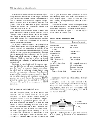
One process step particularly suited for round sub- versions is described in Figure 29.1, and one top gate
strates is photoresist spinning. Square substrates rotating TFT is shown in Exercise 29.3.
5000 rpm create turbulence in the corners, and unifor-
mity cannot be obtained. One solution is to use a round
carrier with a recess for the square substrate. Another Process flow for bottom-gate TFT
solution is to rotate both the substrate and the bowl in
unison, to minimize turbulence. Process Function/comment
Not only are the substrates square, the standardization
Cr deposition Gate metal
of their sizes is almost non-existent. This is difficult for
Gate lithography and Wet etching
process tools and tool automations, in particular. What
etching
is more, thicknesses are not standardized, either. Add to
SiN x deposition Gate dielectric
this the fact that some ceramic substrates have densities
Channel a-Si:H Undoped
three times that of silicon and quartz, and they can be
deposition
2 mm thick, which translates to a factor of a 10 mass
difference. Thickness also has an effect on thermal SiN x deposition S/D separation
equilibrium and the heating of wafers, intentional and SiN x lithography & Plasma etching
unintentional. etching
Substrates of piezoelectric and ferroelectric mate- n+ a-Si:H deposition S/D contact improvement
rials like LiNbO 3 not only pose contamination dan- Cr deposition S/D metal contact
gers, but “react” to processes: plasmas cause charg- Lithography Transistor isolation
ing which leads to mechanical volume changes which Etching Wet etch selective
can relax via unexpected mechanisms. Special material Cr/n+ a-Si:H/a-Si:H against nitride
properties like magnetism or superconductivity depend
on crystalline structure, and sometimes process tem-
peratures are severely limited. For example, PECVD Metallization for row and column address electrodes
◦
protective coatings must be deposited at 120 C, but is not shown.
of course, film quality is not comparable to 300 C Amorphous silicon is the active material in the
◦
deposition. channel and its annealing is one of the crucial steps.
Amorphous (and polycrystalline silicon) have many
dangling bonds, which have to be passivated for long-
29.2 THIN-FILM TRANSISTORS, TFTs term stability. Forming gas anneal (H 2 /N 2 ) at ca. 400 C
◦
is a standard procedure.
Thin-film transistors (TFTs) are MOS devices with
deposited films as channel materials and as gate
dielectrics. The most common channel material is Cr
amorphous silicon, a-Si:H, and sometimes, tempera- SiN
ture allowing, a crystallization process can turn a- x (n ) a-Si:H
+
Si:H into polysilicon, but there is no need to limit Undoped a-Si:H
oneself to silicon: conducting polymers such as pen-
tacenes and thiophenes can be used. However, car- SiN x
rier mobilities of these materials are rather differ- Glass
ent from single-crystal silicon: mobility of SCS is
2
2
ca. 500 cm /Vs, polysilicon ca. 100 cm /Vs, a-Si:H Figure 29.1 Bottom-gate TFT on glass. From Gleskova,
2
ca. 1 cm /Vs and organic molecules between 0.001 H. et al. (2001), by permission of The Electrochemical
2
to 1 cm /Vs. Deposited PECVD oxide or nitride are Society