
Page 325 - Sami Franssila Introduction to Microfabrication
P. 325
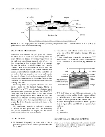
304 Introduction to Microfabrication


                                                     Cr
                              +
                            (n ) a-Si:H                           100 nm
                                                                            ~50 nm
                           Undoped
                           a-Si:H                                            ~200 nm
                                                                                  ~400 nm

                       SiN x
                                                  Polyimide foil                   500 nm


                                                                     ◦
            Figure 29.3 TFT on polyimide; the maximum processing temperature is 150 C. From Gleskova, H. et al. (2001), by
            permission of The Electrochemical Society

            29.2.2 TFTs on other substrates              2. Calculate row and column address electrode resis-
                                                           tances on a 15 in. TFT display. Compare ITO and
            Limitations that hold true for glass plates are also true  real metals.
            for TFTs made on steel foils, even though there are  3. Design a fabrication process for the top gate TFT
            some differences. Higher processing temperatures can  shown below. The maximum process temperature is
            be used from a mechanical strength point of view, but  350 C. From Wu, M. et al. (1999), by permission of
                                                              ◦
            iron contamination is a concern. Steel is a conduct-  AIP.
            ing material and an electrical insulator layer must be
            deposited on it before any electrical devices. Iron con-  AI                     200 nm
            tamination concern replaces the sodium-contamination
            danger, so an ion barrier is needed. If the same film can  SiO 2                  200 nm
            act both as electrical insulation, ion barrier and smooth-  µc-Si n +            75 nm
            ing layer, it is better. Steel surface smoothness is inferior  Polysilicon       160 nm
            to glass, and planarization may be needed. Spin-on-glass                         480 nm
            can fulfill all these disparate requirements and is clearly  Insulaton layer:
            a strong candidate.                          Spin-on glass+SiO 2
              Processing TFTs on polymer substrates sets even  Steel substrate               200 µm
            stricter limits on the thermal budget. Shown in
            Figure 29.3 is a TFT on polyimide substrate. Maxi-
                                                    ◦
            mum processing temperature has been limited to 150 C
            (polyimide thin films on silicon wafers can tolerate  4. TFT itself takes up very little area compared with
                                          ◦
            much higher temperatures, up to 400 C because con-  pixel, and transistor packing density increase offered
            duction to the substrate effectively spreads excess heat).  by self-alignment is not important. What are the
            Plasma nitride serves two important functions: it pas-  benefits of self-alignment in TFT fabrication?
            sivates the device from the substrate and it acts as the  5. What are the integration issues when the RCL passive
            gate dielectric.                               chip in Figure 24.13 and TFBAR in Figure 7.9 are
              The mechanical strength of polyimide substrates  made on:
            is inferior to both glass and steel, but fortunately  (a) Si
            low process temperatures are helpful, and due to low  (b) glass
            temperatures stresses are also minimized.      (c) fused silica.


            29.3 EXERCISES                               REFERENCES AND RELATED READINGS
            1. If flat-panel lithography is done with a 50 µm  Becker, H. et al: Planar quartz chips with submicron channels
               proximity gap, what is the smallest possible linewidth  for two-dimensional capillary electrophoresis applciations, J.
               on an FPD?                                 Micromech. Microeng. 8 (1998), 24.