
Page 324 - Sami Franssila Introduction to Microfabrication
P. 324
Processing on Non-silicon Substrates 303
Thermal oxidation cannot obviously be used but Typical TCOs include indium oxide (In 2 O 3 ) and
all dielectrics are (PE)CVD or sputter deposited. Ion tin oxide (SnO 2 ) and their alloys, such as SnO 2 :F or
implantation damage anneal, which is done at 900 C, In 2 O 3 :Sn, indium tin oxide, known as ITO. Resistivities
◦
cannot be used and implantation is not a very attractive of transparent conducting oxides are 100 to 500 µohm-
technique for large-area microelectronics because it is cm (a factor of 100 higher than that of true metals),
a slow, serial process. Other doping processes, such as which translates to sheet resistances of a few ohms, and
gas-phase doping during PECVD silicon, must be used. to transmission of over 70% from 400 to 1000 nm (with
−1
Activation anneal temperatures are so low that we must absorption coefficient α ≈ 0.04 µm ).
accept only partial activation of dopants. The yield is paramount because there are usually
TFT performance can be improved by the same tech- just a few displays per panel: a 50 cm by 50 cm plate
niques used in silicon MOSFETs, but the low-cost/large- may contain just four displays. Yield statistics are very
area limitations must be borne in mind. Self-aligned different from ICs, which have hundreds of devices
structures have been developed for TFTs with spacers, per wafer (yield will be discussed in Chapter 36 in
lightly doped drains (LDDs) and self-aligned silicides. more detail). Fortunately, linewidths are very relaxed.
CMP cannot be used because of cost considerations However, large areas need to be exposed (and still larger
and large-area limitations, and plasma-etching unifor- ones are required in the future) whereas IC lithography
mity across 50 cm panels can also be problematic. How- benefits from small area exposure. Film thicknesses
ever, because linewidths are of the order of 10 µm, wet are, however, similar to IC fabrication, and particles,
etching is suitable for most etching steps. pinholes and hillocks are dangerous. Killer defect is
If alkali glass is used, sodium contamination is a half the film thickness, which puts high demands on
problem: the very first process step must be an ion cleanroom facilities.
barrier deposition to isolate the silicon devices from
the glass substrate. Aluminum oxide and various other
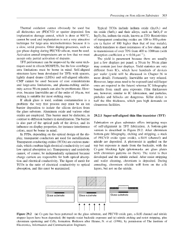
oxides are employed. This barrier must be dielectric, in 29.2.1 Super-self-aligned thin film transistor (TFT)
contrast to diffusion barriers in metallization. The barrier
is also part of the optical path of the device, and its Fabrication on glass substrates offers intriguing ways
influence on display properties, for instance interference of self-alignment in TFT fabrication. A bottom-gate
colors, must be borne in mind. version is described in Figure 29.2. After chromium
In FPDs, depending on the optical design of the dis- bottom-gate lithography, etching and stripping, a stack
play, transparent conductors are used for metallization. of PECVD oxide (gate oxide), a-Si:H (channel) and
Transparent conducting oxides (TCOs) are curious mate- nitride are deposited. A photoresist is applied on the
rials, which combine high electrical conductivity (σ) and top but exposure is made from the backside, with the
low optical absorption (α). Transparency and resistivity Cr-gate blocking light (photomasks are glass plates
cannot, of course, be independently optimized because with chromium patterns on them). The resist is then
charge carriers are responsible for both optical absorp- developed and the nitride etched. After resist stripping
tion and electrical conductivity. The figure of merit for and wafer cleaning, chromium is deposited. During
TCOs is the ratio of electrical conductivity to optical annealing, chromium silicide will form on the a-Si
absorption, and this must be maximized. layers, but not on the nitride.
Glass substrate Glass substrate Glass substrate
Figure 29.2 (a) Cr-gate has been patterned on the glass substrate, and PECVD oxide gate, a-Si:H channel and nitride
stopper layers have been deposited; (b) topside resist backside exposure and (c) nitride etching and resist stripping, plus
chromium sputtering and CrSi 2 formation. Redrawn after Hirano, N. et al. (1996), by permission of The Institute of
Electronics, Information and Communication Engineers