
Page 272 - Sami Franssila Introduction to Microfabrication
P. 272
Process Integration 251
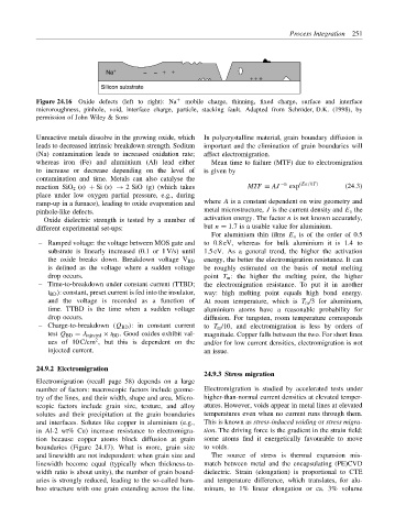
Na + − − + +
+ + +
Silicon substrate
Figure 24.16 Oxide defects (left to right): Na + mobile charge, thinning, fixed charge, surface and interface
microroughness, pinhole, void, interface charge, particle, stacking fault. Adapted from Schr¨ oder, D.K. (1998), by
permission of John Wiley & Sons
Unreactive metals dissolve in the growing oxide, which In polycrystalline material, grain boundary diffusion is
leads to decreased intrinsic breakdown strength. Sodium important and the elimination of grain boundaries will
(Na) contamination leads to increased oxidation rate; affect electromigration.
whereas iron (Fe) and aluminium (Al) lead either Mean time to failure (MTF) due to electromigration
to increase or decrease depending on the level of is given by
contamination and time. Metals can also catalyse the
reaction SiO 2 (s) + Si (s) → 2 SiO (g) (which takes MTF = AJ −n exp (Ea/kT ) (24.3)
place under low oxygen partial pressure, e.g., during
ramp-up in a furnace), leading to oxide evaporation and where A is a constant dependent on wire geometry and
pinhole-like defects. metal microstructure, J is the current density and E a the
Oxide dielectric strength is tested by a number of activation energy. The factor n is not known accurately,
different experimental set-ups: but n = 1.7 is a usable value for aluminium.
For aluminium thin films E a is of the order of 0.5
– Ramped voltage: the voltage between MOS gate and to 0.8 eV, whereas for bulk aluminium it is 1.4 to
substrate is linearly increased (0.1 or 1 V/s) until 1.5 eV. As a general trend, the higher the activation
the oxide breaks down. Breakdown voltage V BD energy, the better the electromigration resistance. It can
is defined as the voltage where a sudden voltage be roughly estimated on the basis of metal melting
drop occurs. point T m : the higher the melting point, the higher
– Time-to-breakdown under constant current (TTBD; the electromigration resistance. To put it in another
t BD ): constant, preset current is fed into the insulator, way: high melting point equals high bond energy.
and the voltage is recorded as a function of At room temperature, which is T m /3 for aluminium,
time. TTBD is the time when a sudden voltage aluminium atoms have a reasonable probability for
drop occurs. diffusion. For tungsten, room temperature corresponds
– Charge-to-breakdown (Q BD ): in constant current to T m /10, and electromigration is less by orders of
test Q BD = J injected × t BD . Good oxides exhibit val- magnitude. Copper falls between the two. For short lines
2
ues of 10 C/cm , but this is dependent on the and/or for low current densities, electromigration is not
injected current. an issue.
24.9.2 Electromigration
24.9.3 Stress migration
Electromigration (recall page 58) depends on a large
number of factors: macroscopic factors include geome- Electromigration is studied by accelerated tests under
try of the lines, and their width, shape and area. Micro- higher-than-normal current densities at elevated temper-
scopic factors include grain size, texture, and alloy atures. However, voids appear in metal lines at elevated
solutes and their precipitation at the grain boundaries temperatures even when no current runs through them.
and interfaces. Solutes like copper in aluminium (e.g., This is known as stress-induced voiding or stress migra-
in Al-2 wt% Cu) increase resistance to electromigra- tion. The driving force is the gradient in the strain field:
tion because copper atoms block diffusion at grain some atoms find it energetically favourable to move
boundaries (Figure 24.17). What is more, grain size to voids.
and linewidth are not independent: when grain size and The source of stress is thermal expansion mis-
linewidth become equal (typically when thickness-to- match between metal and the encapsulating (PE)CVD
width ratio is about unity), the number of grain bound- dielectric. Strain (elongation) is proportional to CTE
aries is strongly reduced, leading to the so-called bam- and temperature difference, which translates, for alu-
boo structure with one grain extending across the line. minum, to 1% linear elongation or ca. 3% volume