
Page 266 - Sami Franssila Introduction to Microfabrication
P. 266
Process Integration 245
Figure 24.9 Coincident structures on two different levels
will lead to serious topography evolution due to misalign-
ment. The spacing rule of unrelated structures must also
account for interlayer thicknesses to avoid crevasses
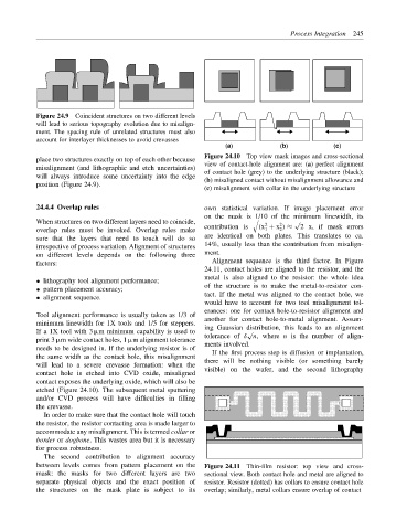
(a) (b) (c)
Figure 24.10 Top view mask images and cross-sectional
place two structures exactly on top of each other because
view of contact-hole alignment are: (a) perfect alignment
misalignment (and lithographic and etch uncertainties)
of contact hole (grey) to the underlying structure (black);
will always introduce some uncertainty into the edge (b) misaligned contact without misalignment allowance and
position (Figure 24.9).
(c) misalignment with collar in the underlying structure
24.4.4 Overlap rules own statistical variation. If image placement error
on the mask is 1/10 of the minimum linewidth, its
When structures on two different layers need to coincide, 2 2 √
overlap rules must be invoked. Overlap rules make contribution is (x + x ) ≈ 2 x, if mask errors
1
2
sure that the layers that need to touch will do so are identical on both plates. This translates to ca.
irrespective of process variation. Alignment of structures 14%, usually less than the contribution from misalign-
on different levels depends on the following three ment.
factors: Alignment sequence is the third factor. In Figure
24.11, contact holes are aligned to the resistor, and the
metal is also aligned to the resistor: the whole idea
• lithography tool alignment performance;
• pattern placement accuracy; of the structure is to make the metal-to-resistor con-
• alignment sequence. tact. If the metal was aligned to the contact hole, we
would have to account for two tool misalignment tol-
erances: one for contact hole-to-resistor alignment and
Tool alignment performance is usually taken as 1/3 of another for contact hole-to-metal alignment. Assum-
minimum linewidth for 1X tools and 1/5 for steppers.
ing Gaussian distribution, this leads to an alignment
If a 1X tool with 3 µm minimum capability is used to √
tolerance of δ n, where n is the number of align-
print 3 µm wide contact holes, 1 µm alignment tolerance
ments involved.
needs to be designed in. If the underlying resistor is of
If the first process step is diffusion or implantation,
the same width as the contact hole, this misalignment
there will be nothing visible (or something barely
will lead to a severe crevasse formation: when the
visible) on the wafer, and the second lithography
contact hole is etched into CVD oxide, misaligned
contact exposes the underlying oxide, which will also be
etched (Figure 24.10). The subsequent metal sputtering
and/or CVD process will have difficulties in filling
the crevasse.
In order to make sure that the contact hole will touch
the resistor, the resistor contacting area is made larger to
accommodate any misalignment. This is termed collar or
border or dogbone. This wastes area but it is necessary
for process robustness.
The second contribution to alignment accuracy
between levels comes from pattern placement on the Figure 24.11 Thin-film resistor: top view and cross-
mask: the masks for two different layers are two sectional view. Both contact hole and metal are aligned to
separate physical objects and the exact position of resistor. Resistor (dotted) has collars to ensure contact hole
the structures on the mask plate is subject to its overlap; similarly, metal collars ensure overlap of contact