
Page 262 - Sami Franssila Introduction to Microfabrication
P. 262
Process Integration 241
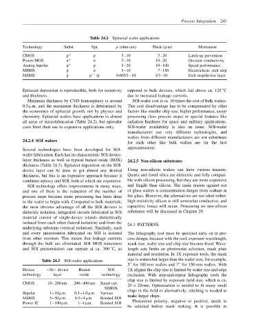
Table 24.2 Epitaxial wafer applications
Technology Subst Epi ρ (ohm-cm) Thick (µm) Motivation
CMOS p + p 5–10 5–20 Latch-up prevention
Power-MOS n + n 5–10 10–20 On-state conductivity
Analog bipolar p + p 1–20 10–100 Speed performance
MEMS p n 1–10 7–150 Electrochem. etch stop
MEMS p p ++ /p 0.005/1–10 3/3–30 Etch stop/device layer
◦
Epitaxial deposition is reproducible, both for resistivity opposed to bulk devices, which fail above ca. 125 C
and thickness. due to increased leakage currents.
Minimum thickness by CVD homoepitaxy is around SOI-wafer cost is ca. 10 times the cost of bulk wafers.
0.5 µm, and the maximum thickness is determined by This cost disadvantage has to be compensated by other
the economics of epitaxial growth, not by physics and factors like smaller chip size, higher performance, easier
chemistry. Epitaxial wafers have applications in almost processing (less process steps) or special features like
all areas of microfabrication (Table 24.2), but epiwafer radiation hardness for space and military applications.
costs limit their use to expensive applications only. SOI-wafer availability is also an issue: SOI-wafer
manufacturers use very different technologies, and
wafers from different manufacturers are not substitutes
24.2.4 SOI wafers
for each other like bulk wafers are (in the first
approximation).
Several technologies have been developed for SOI-
wafer fabrication. Each has its characteristic SOI device-
layer thickness as well as typical buried oxide (BOX) 24.2.5 Non-silicon substrates
thickness (Table 24.3). Epitaxial deposition on the SOI-
device layer can be done to get almost any desired Using non-silicon wafers can have various reasons.
thickness, but this is an expensive approach because it Quartz and fused silica are dielectric and fully compati-
combines epitaxy and SOI, both of which are expensive. ble with silicon processing, but they are more expensive
SOI technology offers improvements in many ways, and fragile than silicon. The main reason against use
and one of them is the reduction of the number of of glass wafers is contamination danger from sodium in
process steps because more processing has been done the glass. However, the alternatives are not ideal either:
to the wafer to begin with. Compared to bulk materials, high-resistivity silicon is still somewhat conductive, and
the most obvious advantage of all the SOI devices is capacitive losses will occur. Processing on non-silicon
dielectric isolation. Integrated circuits fabricated in SOI substrates will be discussed in Chapter 29.
material consist of single-device islands dielectrically
isolated from each other (lateral isolation) and from the
24.3 PATTERNS
underlying substrate (vertical isolation). Similarly, each
and every piezoresistor fabricated on SOI is isolated The lithography tool must be specified early on in pro-
from other resistors. This means that leakage currents cess design, because with the tool, exposure wavelength,
through the bulk are eliminated. SOI MOS transistors mask size, wafer size and chip size become fixed. Wave-
◦
and SOI piezoresistors can operate at ca. 300 C, as length sets limits on photoresist selection, mask plate
material and resolution. In 1X exposure tools, the mask
Table 24.3 SOI-wafer applications size is somewhat larger than the wafer size, for example,
′′
′′
5 for 100 mm wafers and 7 for 150 mm wafers. With
Device <Si> device Buried SOI 1X aligner the chip size is limited by wafer size and edge
technology layer oxide technology exclusion. With step-and-repeat lithography tools the
chip size is limited by exposure field size, which is ca.
CMOS 10–200 nm 200–400 nm Smart-cut,
20 × 20 mm. Optimization is needed to fit many small
SIMOX
Bipolar 1–10 µm 0.1–1.0 µm Various chips in the field or alternatively, stitching is needed to
MEMS 5–50 µm 0.5–4 µm Bonded SOI make larger chips.
Power IC 1–100 µm 1–4 µm Bonded SOI Photoresist polarity, negative or positive, needs to
be selected before mask making. It is possible to