
Page 260 - Sami Franssila Introduction to Microfabrication
P. 260
Process Integration 239
technology <111> is used. When both MOS and Table 24.1 CZ-silicon resistivity ranges
bipolars are on the same chip (BiCMOS), <100> wafers (more extreme values can be obtained but
are used because oxide for the MOS-part is more critical then only part of the ingot will be within
than <111> special features of the bipolar part. If specifications)
there are no special requirements for silicon electrical
or mechanical properties, <100> silicon is usually used Boron 0.002–4000 ohm-cm
Phosphorus
0.001–1000 ohm-cm
because of its wide availability and low cost. Antimony 0.008–0.1 ohm-cm
Crystal orientation need not be exactly along the Arsenic 0.002–0.01 ohm-cm
major axis. Intentional off-axis cut (miscut) is beneficial
for silicon epitaxy. <111> surface is atomically flat
but the miscut introduces terraces that are favourable
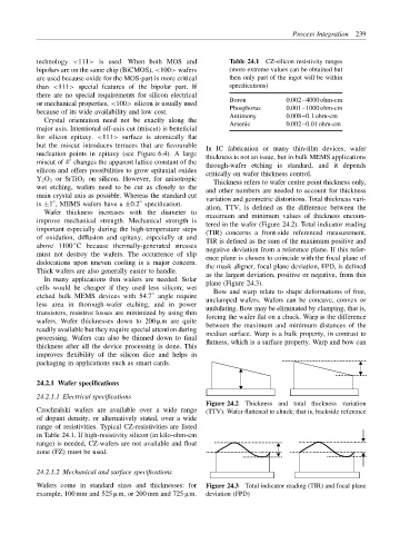
In IC fabrication or many thin-film devices, wafer
nucleation points in epitaxy (see Figure 6.4). A large thickness is not an issue, but in bulk MEMS applications
miscut of 4 changes the apparent lattice constant of the through-wafer etching is standard, and it depends
◦
silicon and offers possibilities to grow epitaxial oxides critically on wafer thickness control.
Y 2 O 3 or SrTiO 3 on silicon. However, for anisotropic Thickness refers to wafer centre point thickness only,
wet etching, wafers need to be cut as closely to the and other numbers are needed to account for thickness
main crystal axis as possible. Whereas the standard cut variation and geometric distortions. Total thickness vari-
◦
is ±1 , MEMS wafers have a ±0.2 specification. ation, TTV, is defined as the difference between the
◦
Wafer thickness increases with the diameter to maximum and minimum values of thickness encoun-
improve mechanical strength. Mechanical strength is tered in the wafer (Figure 24.2). Total indicator reading
important especially during the high-temperature steps (TIR) concerns a front-side referenced measurement.
of oxidation, diffusion and epitaxy, especially at and TIR is defined as the sum of the maximum positive and
◦
above 1100 C because thermally-generated stresses
negative deviation from a reference plane. If this refer-
must not destroy the wafers. The occurrence of slip
ence plane is chosen to coincide with the focal plane of
dislocations upon uneven cooling is a major concern. the mask aligner, focal plane deviation, FPD, is defined
Thick wafers are also generally easier to handle. as the largest deviation, positive or negative, from this
In many applications thin wafers are needed. Solar plane (Figure 24.3).
cells would be cheaper if they used less silicon; wet Bow and warp relate to shape deformations of free,
etched bulk MEMS devices with 54.7 angle require unclamped wafers. Wafers can be concave, convex or
◦
less area in thorough-wafer etching, and in power undulating. Bow may be eliminated by clamping, that is,
transistors, resistive losses are minimized by using thin forcing the wafer flat on a chuck. Warp is the difference
wafers. Wafer thicknesses down to 200 µm are quite between the maximum and minimum distances of the
readily available but they require special attention during median surface. Warp is a bulk property, in contrast to
processing. Wafers can also be thinned down to final
flatness, which is a surface property. Warp and bow can
thickness after all the device processing is done. This
improves flexibility of the silicon dice and helps in
packaging in applications such as smart cards.
24.2.1 Wafer specifications
24.2.1.1 Electrical specifications
Figure 24.2 Thickness and total thickness variation
Czochralski wafers are available over a wide range (TTV). Wafer flattened to chuck; that is, backside reference
of dopant density, or alternatively stated, over a wide
range of resistivities. Typical CZ-resistivities are listed
in Table 24.1. If high-resistivity silicon (in kilo-ohm-cm
range) is needed, CZ-wafers are not available and float
zone (FZ) must be used.
24.2.1.2 Mechanical and surface specifications
Wafers come in standard sizes and thicknesses: for Figure 24.3 Total indicator reading (TIR) and focal plane
example, 100 mm and 525 µm, or 200 mm and 725 µm. deviation (FPD)