
Page 250 - Sami Franssila Introduction to Microfabrication
P. 250
Structures by Deposition 229
(a) (b)
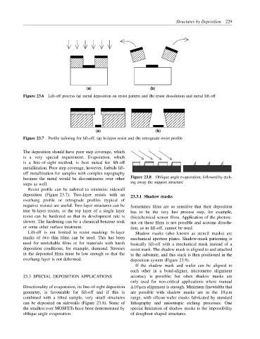
Figure 23.6 Lift-off process (a) metal deposition on resist pattern and (b) resist dissolution and metal lift-off
(a) (b)
Figure 23.7 Profile tailoring for lift-off: (a) bi-layer resist and (b) retrograde resist profile
The deposition should have poor step coverage, which
is a very special requirement. Evaporation, which
is a line-of-sight method, is best suited for lift-off
metallization. Poor step coverage, however, forbids lift-
off metallization for samples with complex topography
because the metal would be discontinuous over other Figure 23.8 Oblique angle evaporation; followed by etch-
steps as well. ing away the support structure
Resist profile can be tailored to minimize sidewall
deposition (Figure 23.7). Two-layer resists with an 23.3.1 Shadow masks
overhang profile or retrograde profiles (typical of
negative resists) are useful. Two-layer structures can be Sometimes films are so sensitive that their deposition
true bi-layer resists, or the top layer of a single layer has to be the very last process step, for example,
resist can be hardened so that its development rate is (bio)chemical sensor films. Application of the photore-
slower. The hardening can be a chemical benzene soak sist on these films is not possible and acetone dissolu-
or some other surface treatment. tion, as in lift-off, cannot be used.
Lift-off is not limited to resist masking: bi-layer Shadow masks (also known as stencil masks) are
masks of two thin films can be used. This has been mechanical aperture plates. Shadow-mask patterning is
used for unetchable films or for materials with harsh basically lift-off with a mechanical mask instead of a
deposition conditions, for example, diamond. Stresses resist mask. The shadow mask is aligned to and attached
in the deposited films must be low enough so that the to the substrate, and this stack is then positioned in the
overhang layer is not deformed. deposition system (Figure 23.9).
If the shadow mask and wafer can be aligned to
each other in a bond-aligner, micrometre alignment
23.3 SPECIAL DEPOSITION APPLICATIONS accuracy is possible; but often shadow masks are
only used for non-critical applications where manual
Directionality of evaporation, its line-of-sight deposition ±10 µm alignment is enough. Minimum linewidths that
geometry, is favourable for lift-off and if this is are possible with shadow masks are in the 10 µm
combined with a tilted sample, very small structures range, with silicon-wafer masks fabricated by standard
can be deposited on sidewalls (Figure 23.8). Some of lithography and anisotropic etching processes. One
the smallest ever MOSFETs have been demonstrated by special limitation of shadow masks is the impossibility
oblique angle evaporation. of doughnut-shaped structures.