
Page 50 - Sami Franssila Introduction to Microfabrication
P. 50
Simulation of Microfabrication Processes 29
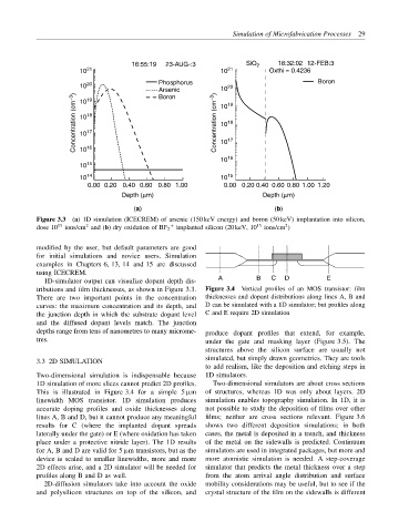
16:55:19 23-AUG-:3 SiO 2 18:32:02 12-FEB:3
10 21 10 21 Oxthi = 0.4236
10 20 Phosphorus 20 Boron
Arsenic 10 19
Boron
Concentration (cm −3 ) 10 18 Concentration (cm −3 ) 10 18
19
10
10
17
10
17
10
16
10
10 16
10 15
10 14 10 15
0.00 0.20 0.40 0.60 0.80 1.00 0.00 0.20 0.40 0.60 0.80 1.00 1.20
Depth (µm) Depth (µm)
(a) (b)
Figure 3.3 (a) 1D simulation (ICECREM) of arsenic (150 keV energy) and boron (50 keV) implantation into silicon,
2
2
dose 10 15 ions/cm and (b) dry oxidation of BF 2 + implanted silicon (20 keV, 10 15 ions/cm )
modified by the user, but default parameters are good
for initial simulations and novice users. Simulation
examples in Chapters 6, 13, 14 and 15 are discussed
using ICECREM.
1D-simulator output can visualize dopant depth dis- A B C D E
tributions and film thicknesses, as shown in Figure 3.3. Figure 3.4 Vertical profiles of an MOS transistor: film
There are two important points in the concentration thicknesses and dopant distributions along lines A, B and
curves: the maximum concentration and its depth, and D can be simulated with a 1D simulator; but profiles along
the junction depth in which the substrate dopant level C and E require 2D simulation
and the diffused dopant levels match. The junction
depths range from tens of nanometres to many microme- produce dopant profiles that extend, for example,
tres. under the gate and masking layer (Figure 3.5). The
structures above the silicon surface are usually not
simulated, but simply drawn geometries. They are tools
3.3 2D SIMULATION
to add realism, like the deposition and etching steps in
Two-dimensional simulation is indispensable because 1D simulators.
1D simulation of more slices cannot predict 2D profiles. Two-dimensional simulators are about cross sections
This is illustrated in Figure 3.4 for a simple 5 µm of structures, whereas 1D was only about layers. 2D
linewidth MOS transistor. 1D simulation produces simulation enables topography simulation. In 1D, it is
accurate doping profiles and oxide thicknesses along not possible to study the deposition of films over other
lines A, B and D, but it cannot produce any meaningful films; neither are cross sections relevant. Figure 3.6
results for C (where the implanted dopant spreads shows two different deposition simulations: in both
laterally under the gate) or E (where oxidation has taken cases, the metal is deposited in a trench, and thickness
place under a protective nitride layer). The 1D results of the metal on the sidewalls is predicted. Continuum
for A, B and D are valid for 5 µm transistors, but as the simulators are used in integrated packages, but more and
device is scaled to smaller linewidths, more and more more atomistic simulation is needed. A step-coverage
2D effects arise, and a 2D simulator will be needed for simulator that predicts the metal thickness over a step
profiles along B and D as well. from the atom arrival angle distribution and surface
2D-diffusion simulators take into account the oxide mobility considerations may be useful, but to see if the
and polysilicon structures on top of the silicon, and crystal structure of the film on the sidewalls is different