
Page 53 - Sami Franssila Introduction to Microfabrication
P. 53
32 Introduction to Microfabrication
REFERENCES AND RELATED READINGS
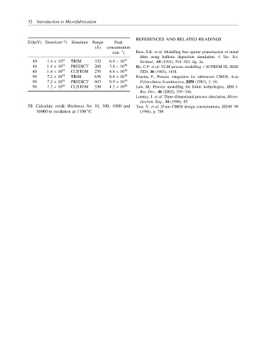
−2
E/(keV) Dose/(cm ) Simulator Range Peak
( ˚ A) concentration
−3
(cm ) Dew, S.K. et al: Modelling bias sputter planarization of metal
films using ballistic deposition simulation, J. Vac. Sci.
40 1.4 × 10 13 TRIM 332 6.0 × 10 17 Technol., A9 (1991), 519–523, fig. 2a.
40 1.4 × 10 13 PREDICT 268 3.8 × 10 18 Ho, C.P. et al: VLSI process modelling – SUPREM III, IEEE
40 1.4 × 10 13 CUSTOM 270 4.6 × 10 18 TED, 30 (1983), 1438.
90 7.2 × 10 14 TRIM 636 8.6 × 10 18 Krusius, P., Process integration for submicron CMOS, Acta
90 7.2 × 10 14 PREDICT 603 9.9 × 10 19 Polytechnica Scandinavica, El58 (1987), 1–16.
90 7.2 × 10 14 CUSTOM 530 1.2 × 10 20 Law, M.: Process modelling for future technologies, IBM J.
Res. Dev., 46 (2002), 339–346.
Lorentz, J. et al: Three-dimensional process simulation, Micro-
electron. Eng., 34 (1996), 85.
5S. Calculate oxide thickness for 10, 100, 1000 and Taur, Y. et al: 25 nm CMOS design considerations, IEDM ’98
10 000 m oxidation at 1100 C. (1998), p. 789.
◦