
Page 58 - Sami Franssila Introduction to Microfabrication
P. 58
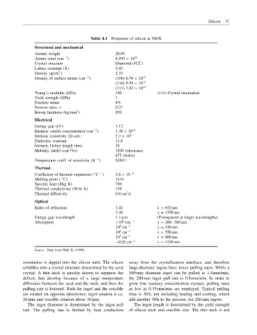
Silicon 37


                                       Table 4.1  Properties of silicon at 300 K
               Structural and mechanical
               Atomic weight                     28.09
                            −3
               Atoms, total (cm )                4.995 × 10 22
               Crystal structure                 Diamond (FCC)
               Lattice constant ( ˚ A)           5.43
                          3
               Density (g/cm )                   2.33
                                     −2
               Density of surface atoms (cm )    (100) 6.78 × 10 14
                                                 (110) 9.59 × 10 14
                                                 (111) 7.83 × 10 14
               Young’s modulus (GPa)             190               (111) Crystal orientation
               Yield strength (GPa)              7
               Fracture strain                   4%
               Poisson ratio, ν                  0.27
                                 2
               Knoop hardness (kg/mm )           850
               Electrical
               Energy gap (eV)                   1.12
                                        −3
               Intrinsic carrier concentration (cm )  1.38 × 10 10
               Intrinsic resistivity ( -cm)      2.3 × 10 5
               Dielectric constant               11.8
               Intrinsic Debye length (nm)       24
                              2
               Mobility (drift) (cm /Vs)         1500 (electrons)
                                                 475 (holes)
                                         −1
               Temperature coeff. of resistivity (K )  0.0017
               Thermal
                                        ◦
                                          −1
               Coefficient of thermal expansion ( C )  2.6 × 10 −6
                           ◦
               Melting point ( C)                1414
               Specific heat (J/kg K)             700
               Thermal conductivity (W/m K)      150
                                                      2
               Thermal diffusivity               0.8 cm /s
               Optical
               Index of refraction               3.42              λ = 632 nm
                                                 3.48              λ = 1550 nm
               Energy gap wavelength             1.1 µm            (Transparent at larger wavelengths)
                                                    6
               Absorption                        >10 cm −1         λ = 200–360 nm
                                                   5
                                                 10 cm −1          λ = 420 nm
                                                   4
                                                 10 cm −1          λ = 550 nm
                                                   3
                                                 10 cm −1          λ = 800 nm
                                                 <0.01 cm −1       λ = 1550 nm
               Source: Data from Hull, R. (1999)
           orientation is dipped into the silicon melt. The silicon  away from the crystallization interface, and therefore
           solidifies into a crystal structure determined by the seed  large-diameter ingots have lower pulling rates. While a
           crystal. A thin neck is quickly drawn to suppress the  100 mm diameter ingot can be pulled at 1.4 mm/min,
           defects that develop because of a large temperature  the 200 mm ingot pull rate is 0.8 mm/min. In order to
           difference between the seed and the melt, and then the  grow low vacancy concentration crystals, pulling rates
           pulling rate is lowered. Both the ingot and the crucible  as low as 0.35 mm/min are employed. Typical pulling
           are rotated (in opposite directions); ingot rotation is ca.  time is 30 h, not including heating and cooling, which
           20 rpm and crucible rotation about 10 rpm.  add another 30 h to the process, for 200 mm ingots.
             The ingot diameter is determined by the ingot pull  The ingot length is determined by the yield strength
           rate. The pulling rate is limited by heat conduction  of silicon neck and crucible size. The thin neck is not