
Page 61 - Sami Franssila Introduction to Microfabrication
P. 61
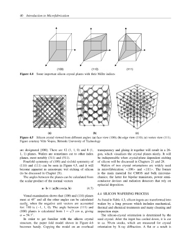
40 Introduction to Microfabrication


                                  (100)              (110)               (111)
            Figure 4.4 Some important silicon crystal planes with their Miller indices


                            (a)                       (b)                     (c)
            Figure 4.5 Silicon crystal viewed from different angles: (a) face view (100); (b) edge view (110); (c) vertex view (111).
            Figure courtesy Ville Voipio, Helsinki University of Technology

            are designated {100}. There are 12 (1, 1, 0) and 8 (1,  transparency and gluing it together will result in a 26-
            1, 1) planes. Wafers are sometimes cut to other index  gon, which visualizes the crystal planes nicely. It will
            planes, most notably (311) and (511).        be indispensable when crystal-plane dependent etching
              Fourfold symmetry of (100) and sixfold symmetry of  of silicon will be discussed in Chapters 21 and 28.
            (110) and (111) can be seen in Figure 4.5, and it will  Wafers of two crystal orientations are widely used
            become apparent in anisotropic wet etching of silicon  in microfabrication: <100> and <111>. The former
            (to be discussed in Chapter 21).             is the main material for CMOS and bulk microme-
              The angles between the planes can be calculated from  chanics; the latter for bipolar transistors, power semi-
            the scalar product of the normal vectors     conductor devices and radiation detectors that rely on
                                                         epitaxial deposition.
                         a · b = |a||b| cos(a, b)  (4.7)
                                                         4.4 SILICON WAFERING PROCESS
              Visual examination shows that (100) and (110) planes
                     ◦
            meet at 45 and all the other angles can be calculated  As listed in Table 4.3, silicon ingots are transformed into
            easily, when the negative unit vectors are accounted  wafers by a long process which includes mechanical,
            for: 110 is (−1, 1, 0). The angle between (111) and  thermal and chemical treatments and many cleaning and
                                         √
            (100) planes is calculated from 1 =  3 cos α, giving  inspection steps.
            α = 54.7 .                                     The silicon-crystal orientation is determined by the
                   ◦
              In order to get familiar with the silicon crystal  seed crystal. After the ingot has cooled down, it is cut
            structure, the paper fold model shown in Figure 4.6  to ca. 50 cm stocks, which are measured for crystal
            becomes handy. Copying the model on an overhead  orientation by X-ray diffraction. A flat or a notch is