
Page 64 - Sami Franssila Introduction to Microfabrication
P. 64
Silicon 43
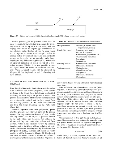
<Si>
SiO 2
<Si>
<Si> <Al O >
2
3
Figure 4.9 Silicon-on-insulator SOI (silicon/oxide/silicon) and SOS (silicon-on-sapphire) wafers
Further processing of the polished wafers leads to Table 4.6 Sources of non-idealities in silicon wafers
more specialized wafers. Epitaxy is a process for grow-
ing more silicon on top of a silicon wafer, with the EGS polysilicon Dopants (B, P) and other
doping level and/or the dopant type independent of impurities (C, metals)
Czochralski growth Impurities from quartz
the substrate wafer. Bonding of two (or even more) Oxygen from quartz
wafers together to create more complex wafers is Carbon from graphite and SiC
another further development. Silicon-on-insulator (SOI) Vacancies and interstitials
wafers can be made by, for example, wafer bond- Precipitates
ing (Figure 4.9). Silicon-on-sapphire (SOS) wafers rely Dislocations
on epitaxial deposition of silicon on top of a crys- Wafering process Contamination from tools
talline sapphire (Al 2 O 3 ). It is also possible to cre- Mechanical distortions
ate layers inside the wafer for additional function- Wafer processing Contamination
ality. These advanced wafers will be discussed in Crystallinity defects
Chapters 15 (Ion implantation) and 17 (Bonding and Precipitation
layer transfer). Mechanical distortions
Dislocations
4.5 DEFECTS AND NON-IDEALITIES IN SILICON
can be much higher because fabrication steps introduce
CRYSTALS
more iron.
Point defects are zero-dimensional: vacancies (miss-
Even though silicon-wafer fabrication results in wafers
with extremely well-defined properties, some defects ing atoms in the lattice), substitutional impurities (for-
are bound to be found. These defects can be classified eign atoms at silicon lattice sites) and interstitials (atoms
according to their origin as grown-in defects and such as oxygen at non-lattice sites) (Figure 4.10). Diva-
process-induced defects. The former are starting material cancies and phosphorous-vacancy pairs are also point-
and crystal-pulling related, and the latter result from like defects. Point defects play an important role in
the wafering process (at the wafer manufacturer) diffusion, which is obvious because solid diffusion
and from the wafer processing (in the wafer fab) requires empty sites for atoms to move in the lat-
(Table 4.6). tice. Some vacancies are present even at room tem-
Metallic impurities come from polysilicon, quartz perature as a result of thermal equilibrium processes
crucible, graphite and other hot parts of the growth but additional vacancies generated by energetic or high
system. The segregation coefficients of most metals temperature processing play a dominant role in diffu-
are very small, and the crystal is purified relative sion.
to the melt. Metals are, however, fast diffusers in One-dimensional or line defects are called disloca-
silicon, and they react with other defects and form tions. These come in many varieties, for example, extra
half-planes inserted between the regular atomic planes.
clusters. Metals affect electronic devices by creating The order of magnitude of thermally generated stress σ
trapping centres in silicon midgap, reducing minority can be gauged by Equation (4.8):
carrier lifetimes and lowering mobility. Metals can also
precipitate at Si/SiO 2 interface and reduce the oxide σ = αE T (4.8)
quality, as will be discussed in Chapter 24. The allowed
10
iron level in silicon wafers is limited to 10 cm −3 where strain, ε = α T α, depends on the silicon coef-
(starting material limit) but at the end of an IC precess it ficient of thermal expansion, Young’s modulus E (at