
Page 69 - Sami Franssila Introduction to Microfabrication
P. 69
48 Introduction to Microfabrication
Table 5.1 Materials in microfabrication
Conducting Semiconducting Insulating
Elements Al, Cu, W, Mo, Ti Si, Ge Diamond
Oxides RuO 2 SnO 2 SiO 2 , Al 2 O 3 , HfO 2
Nitrides TiN, TaN, W 2 N GaN Si 3 N 4 , AlN, BN
Others TiSi 2 , Al 12 W SiC, GaAs, InP Polymers
Table 5.2 Properties of sputtered molybdenum
Material/thickness Underlayer Conditions Resistivity
Bulk – – 5.6 µohm-cm
Thin film, 50 nm SiO 2 System 1, RT 17 µohm-cm
Thin film, 300 nm SiO 2 System 1, RT 12 µohm-cm
Thin film, 300 nm TiW System 1, RT 9 µohm-cm
Thin film, 300 nm SiO 2 System 2, RT 15 µohm-cm
◦
Thin film, 300 nm SiO 2 System 3, 150 C 9 µohm-cm
◦
Thin film, 300 nm SiO 2 System 3, 450 C 8 µohm-cm
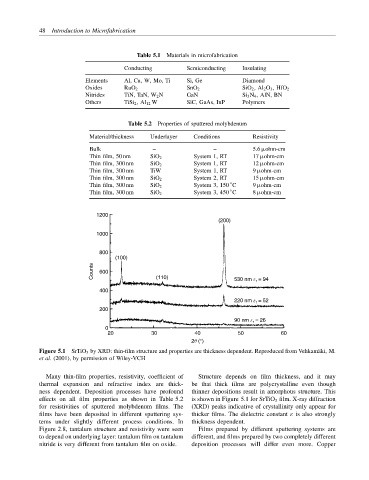
1200
(200)
1000
800
(100)
Counts 600 (110) 530 nm e r = 94
400
220 nm e r = 52
200
90 nm e r = 26
0
20 30 40 50 60
2q (°)
Figure 5.1 SrTiO 3 by XRD: thin-film structure and properties are thickness dependent. Reproduced from Vehkam¨ aki, M.
et al. (2001), by permission of Wiley-VCH
Many thin-film properties, resistivity, coefficient of Structure depends on film thickness, and it may
thermal expansion and refractive index are thick- be that thick films are polycrystalline even though
ness dependent. Deposition processes have profound thinner depositions result in amorphous structure. This
effects on all film properties as shown in Table 5.2 is shown in Figure 5.1 for SrTiO 3 film. X-ray diffraction
for resistivities of sputtered molybdenum films. The (XRD) peaks indicative of crystallinity only appear for
films have been deposited in different sputtering sys- thicker films. The dielectric constant ε is also strongly
tems under slightly different process conditions. In thickness dependent.
Figure 2.8, tantalum structure and resistivity were seen Films prepared by different sputtering systems are
to depend on underlying layer: tantalum film on tantalum different, and films prepared by two completely different
nitride is very different from tantalum film on oxide. deposition processes will differ even more. Copper