
Page 72 - Sami Franssila Introduction to Microfabrication
P. 72
Thin-film Materials and Processes 51
and it reduces the flux of particles to the substrate. (Y b /Y a )(X a /X b ). A steady state situation develops and
Lower flux means a lower deposition rate, but lower composition remains unchanged.
energy leads to less re-sputtering of the film. This
re-sputtering can sometimes be very useful, and it
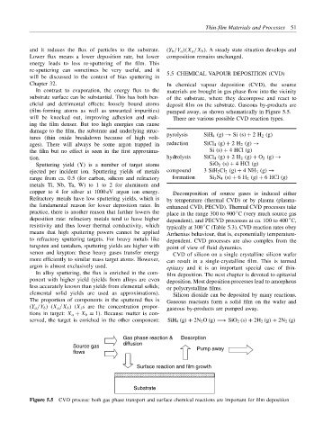
will be discussed in the context of bias sputtering in 5.5 CHEMICAL VAPOUR DEPOSITION (CVD)
Chapter 32. In chemical vapour deposition (CVD), the source
In contrast to evaporation, the energy flux to the materials are brought in gas phase flow into the vicinity
substrate surface can be substantial. This has both ben- of the substrate, where they decompose and react to
eficial and detrimental effects: loosely bound atoms deposit film on the substrate. Gaseous by-products are
(film-forming atoms as well as unwanted impurities) pumped away, as shown schematically in Figure 5.5.
will be knocked out, improving adhesion and mak- There are various possible CVD reaction types.
ing the film denser. But too high energies can cause
damage to the film, the substrate and underlying struc-
tures (thin oxide breakdown because of high volt- pyrolysis SiH 4 (g) → Si (s) + 2 H 2 (g)
ages). There will always be some argon trapped in reduction SiCl 4 (g) + 2 H 2 (g) →
the film but no effect is seen in the first approxima- Si (s) + 4 HCl (g)
tion. hydrolysis SiCl 4 (g) + 2 H 2 (g) + O 2 (g) →
Sputtering yield (Y) is a number of target atoms SiO 2 (s) + 4 HCl (g)
ejected per incident ion. Sputtering yields of metals compound 3 SiH 2 Cl 2 (g) + 4 NH 3 (g) →
range from ca. 0.5 (for carbon, silicon and refractory formation Si 3 N 4 (s) + 6 H 2 (g) + 6 HCl (g)
metals Ti, Nb, Ta, W) to 1 to 2 for aluminum and
copper to 4 for silver at 1000 eV argon ion energy. Decomposition of source gases is induced either
Refractory metals have low sputtering yields, which is by temperature (thermal CVD) or by plasma (plasma-
the fundamental reason for lower deposition rates. In enhanced CVD, PECVD). Thermal CVD processes take
practice, there is another reason that further lowers the place in the range 300 to 900 C (very much source gas
◦
deposition rate: refractory metals tend to have higher dependent), and PECVD processes at ca. 100 to 400 C,
◦
resistivity and thus lower thermal conductivity, which typically at 300 C (Table 5.3). CVD reaction rates obey
◦
means that high sputtering powers cannot be applied Arrhenius behaviour, that is, exponentially temperature-
to refractory sputtering targets. For heavy metals like dependent. CVD processes are also complex from the
tungsten and tantalum, sputtering yields are higher with point of view of fluid dynamics.
xenon and krypton: these heavy gases transfer energy CVD of silicon on a single crystalline silicon wafer
more efficiently to similar mass target atoms. However, can result in a single-crystalline film. This is termed
argon is almost exclusively used. epitaxy and it is an important special case of thin-
In alloy sputtering, the flux is enriched in the com- film deposition. The next chapter is devoted to epitaxial
ponent with higher yield (yields from alloys are even deposition. Most deposition processes lead to amorphous
less accurately known than yields from elemental solids; or polycrystalline films.
elemental solid yields are used as approximations). Silicon dioxide can be deposited by many reactions.
The proportion of components in the sputtered flux is Gaseous reactants form a solid film on the wafer and
(Y a /Y b ) (X a /X b ) (X i s are the concentration propor- gaseous by-products are pumped away.
tions in target: X a + X b = 1). Because matter is con-
served, the target is enriched in the other component: SiH 4 (g) + 2N 2 O (g) −→ SiO 2 (s) + 2H 2 (g) + 2N 2 (g)
Gas phase reaction & Desorption
Source gas diffusion Pump away
flows
Surface reaction and film growth
Substrate
Figure 5.5 CVD process: both gas phase transport and surface chemical reactions are important for film deposition