
Page 70 - Sami Franssila Introduction to Microfabrication
P. 70
Thin-film Materials and Processes 49
films made by sputtering, evaporation, electroplating or
open source resistive heating → thermal evaporation
chemical vapour deposition (CVD) can have a factor
electron beam heating → e-beam evaporation
of 2 differences in resistivity or grain size. When an
equilibrium source heating → molecular beam
amorphous film is annealed at high temperature, it will
epitaxy (MBE)
crystallize. But its crystal size and crystal orientation,
argon ion bombardment → sputtering
and surface roughness will be different from a film
that was initially polycrystalline, even though the films laser beam bombardment → ablation
received identical anneals.
Very thin films are discontinuous and the thickness Shutter blades can be used to prevent deposition on
required for continuous films is process- and material- the wafers during unstable flux (e.g., at the start of the
dependent. One criterion is transparency, which can be deposition or during parameter ramping). Shutter blades
calculated from Lambert’s law: enable very accurate and abrupt interfaces to be made,
almost at the atomic thickness limit.
I = I o exp(−αx) = I o exp(−4πkx/λ) (5.1)
5.3 EVAPORATION AND MOLECULAR
With extinction coefficient (k) values 2 to 6 for metal BEAM EPITAXY
films in the visible range, this translates to ca. 10 to
Evaporation of elemental metals is fairly straightfor-
20 nm as a limit for transparency when a 1/e intensity
ward: heated metals have high vapour pressures and in
drop is used as a criterion.
high vacuum (HV), the evaporated atoms will be trans-
ported to the substrate (Figure 5.3). Atoms arrive at ther-
mal speeds, which results in basically room-temperature
5.2 PHYSICAL VAPOUR DEPOSITION (PVD)
deposition. Evaporation systems are either high-vacuum
(HV) or ultra high–vacuum (UHV) systems, with the
Physical vapour deposition is the dominant method for −11
best UHV deposition systems with 10 Torr base pres-
metallic thin-film deposition. All aluminum films in −12
sures, and 10 Torr oxygen partial pressures.
microfabrication are deposited by PVD, and PVD is used
There are very few parameters in evaporation that
for copper, refractory metals and for metal alloys and can be used to tailor film properties. There is no bom-
compounds like TiW, WN, TiN, MoSi 2 , ZnO and AlN. bardment in addition to thermalized atoms themselves,
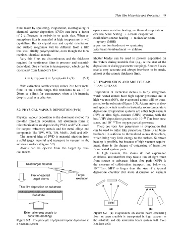
The general idea of PVD is material ejection from which bring very little energy to the surface. Substrate
a solid target material and transport in vacuum to the heating is possible, but because of high vacuum require-
substrate surface (Figure 5.2). ment, there is the danger of outgassing of impurities
Atoms can be ejected from the target by vari- from heated system parts.
ous means. In high vacuum, the atoms do not experience
collisions, and therefore they take a line-of-sight route
from source to substrate. Mean free path (MFP) is
Solid target material the measure of collisionless transport, and below ca.
10 −4 Torr, MFP is larger than the size of a typical
deposition chamber (for more discussion on vacuum
Flux of ejected Target
target atoms excitation
Thin film deposition on substrate
Substrate
(a) (b)
External energy supply to Figure 5.3 (a) Evaporation: an atomic beam emanating
substrate (heating) from an open crucible is transported in high vacuum to
Figure 5.2 The principle of physical vapour deposition in the substrate and (b) molecular beam system with three
a vacuum system Knudsen cells