
Page 65 - Sami Franssila Introduction to Microfabrication
P. 65
44 Introduction to Microfabrication
to a particle. Vacancy clusters were therefore classified
f g h i
as particles, and were given the name COP, for
Crystal Originated Particles (today, advanced multiangle
scatterometry tools can distinguish voids from particles).
It was the fact that the number of COPs did not decrease
in cleaning (and it could in fact increase!) that lead to a
reassessment of their nature. Typical COP sizes are 50
to 200 nm, and they are found in concentrations of 10 4
−3
6
to 10 cm .
Haze is defined as light scattering from surface
defects, for example, scratches, surface roughness or
crystal defects. Haze measurement is by done by
scatterometry, and the whole wafer is scanned in haze
measurement, in contrast to roughness measurement,
a b c d e
which is local area measurement only, for instance,
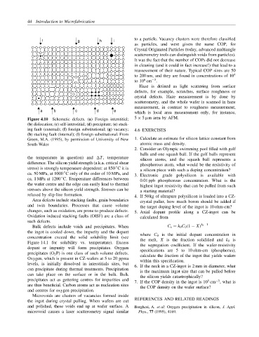
Figure 4.10 Schematic defects. (a) Foreign interstitial; 5 × 5 µm area by AFM.
(b) dislocation; (c) self-interstitial; (d) precipitate; (e) stack-
ing fault (external); (f) foreign substitutional; (g) vacancy; 4.6 EXERCISES
(h) stacking fault (internal); (i) foreign substitutional. From
Green, M.A. (1995), by permission of University of New 1. Calculate an estimate for silicon lattice constant from
South Wales atomic mass and density.
2. Consider an Olympic swimming pool filled with golf
balls and one squash ball. If the golf balls represent
the temperature in question) and T , temperature
silicon atoms, and the squash ball represents a
difference. The silicon yield strength (a.k.a. critical shear phosphorous atom, what would be the resistivity of
◦
stress) is strongly temperature dependent: at 850 C it is a silicon piece with such a doping concentration?
◦
ca. 50 MPa, at 1000 C only of the order of 10 MPa, and 3. Electronic grade polysilicon is available with
◦
ca. 1 MPa at 1200 C. Temperature differences between
0.01 ppb phosphorous concentration. What is the
the wafer centre and the edge can easily lead to thermal
highest ingot resistivity that can be pulled from such
stresses above the silicon yield strength. Stresses can be a starting material?
relaxed by slip-line formation. 4. If 50 kg of ultrapure polysilicon is loaded into a CZ-
Area defects include stacking faults, grain boundaries crystal puller, how much boron should be added if
and twin boundaries. Processes that cause volume the target doping level of the ingot is 10 ohm-cm?
changes, such as oxidation, are prone to produce defects. 5. Axial dopant profile along a CZ-ingot can be
Oxidation induced stacking faults (OISF) are a class of calculated from
such defects.
Bulk defects include voids and precipitates. When C s = k 0 C 0 (1 − X) k 0 −1
the ingot is cooled down, the impurity and the dopant where C 0 is the initial dopant concentration in
concentration exceed the solid solubility limit (see the melt, X is the fraction solidified and k 0 is
Figure 14.1 for solubility vs. temperature). Excess the segregation coefficient. If the wafer-resistivity
dopant or impurity will form precipitates. Oxygen specifications are 5 to 10 ohm-cm (phosphorus),
precipitates (O 2 P) is one class of such volume defects. calculate the fraction of the ingot that yields wafers
Oxygen, which is present in CZ-wafers at 5 to 20 ppma within this specification.
levels, is initially dissolved in interstitials sites, but 6. If the neck in a CZ-ingot is 2 mm in diameter, what
can precipitate during thermal treatments. Precipitation is the maximum ingot size that can be pulled before
can take place on the surface or in the bulk. Bulk the silicon yields catastrophically?
precipitates act as gettering centres for impurities and 7. If the COP density in the ingot is 10 cm , what is
−3
5
are thus beneficial. Carbon atoms act as nucleation sites the COP density on the wafer surface?
and centres for oxygen precipitation.
Microvoids are clusters of vacancies formed inside
the ingot during crystal pulling. When wafers are cut REFERENCES AND RELATED READINGS
and polished, these voids end up at wafer surface. A Borghesi, A. et al: Oxygen precipitation in silicon, J. Appl.
microvoid causes a laser scatterometry signal similar Phys., 77 (1995), 4169.