
Page 60 - Sami Franssila Introduction to Microfabrication
P. 60
Silicon 39
will be of different thicknesses, and this leads to radial according to Equation (4.6)
dopant non-uniformity. There are also stochastic thermal
28 29 29 −
fluctuations in the melt, and these lead to local resistivity n + Si −→ Si −→ P + e (4.6)
variations. Some dopants (As, Sb; and oxygen also) are
A silicon nucleus captures a neutron, and the newly
volatilized from the melt; therefore, concentration along
formed nucleus decays by β-decay. This doping method
the crystal axis is dependent on the gas flow in the
explains why high resistivity silicon (5–20 kohm-cm) is
crystal puller.
available in n-type.
On the other hand, the concentration of oxygen
decreases as the pulling advances. This has to do
with the decreased contact area between the melt and 4.3 SILICON CRYSTAL STRUCTURE
the quartz crucible, and also with the flow patterns
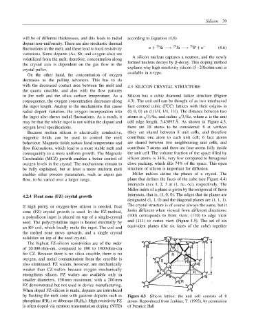
in the melt and the silica surface temperature. As a Silicon has a cubic diamond lattice structure (Figure
consequence, the oxygen concentration decreases along 4.3). The unit cell can be thought of as two interleaved
the ingot length. Analog to the mechanisms that cause face centred cubic (FCC) lattices with their origins in
radial dopant variation, the oxygen incorporation into (0, 0, 0) an d (1/4, 1/4, 1/4). The distance between two
√ √
the ingot also shows radial fluctuations. As a result, it atoms is 3/4a, and radius 3/8a, where a is the unit
may be that the whole ingot is not within the dopant and cell edge length, 5.43095 ˚ A. As shown in Figure 4.3,
oxygen level specifications. there are 18 atoms to be considered: 8 at vertices
Because molten silicon is electrically conductive, (they are shared between 8 unit cells, and therefore
magnetic fields can be used to control the melt contribute one atom to each unit cell; 6 face atoms
behaviour. Magnetic fields reduce local temperature and are shared between two neighbouring unit cells, and
flow fluctuations, which lead to a more stable melt and contribute 3 atoms and there are four atoms fully inside
consequently to a more uniform growth. The Magnetic the unit cell. The volume fraction of the space filled by
Czochralski (MCZ) growth enables a better control of silicon atoms is 34%, very low compared to hexagonal
oxygen levels in the crystal. The mechanisms remain to close packing, which fills 74% of the space. This open
be fully explained, but at least a more uniform melt structure of silicon is important for diffusion.
enables other process parameters, such as argon gas Miller indices define the planes of a crystal. The
flow, to be varied over a larger range. plane that defines the faces of the cube (see Figure 4.4)
intersects axes 1, 2, 3 at (1, ∞, ∞), respectively. The
Miller index of a plane is given by the reciprocal of these
intersects, that is, (1, 0, 0). The edges that tie planes are
4.2.4 Float zone (FZ) crystal growth
designated (1, 1, 0) and the diagonal planes are (1, 1, 1).
The crystal structure is of course always the same, but it
If high purity or oxygen-free silicon is needed, float
looks different when viewed from different directions:
zone (FZ) crystal growth is used. In the FZ-method,
(100) corresponds to front view; (110) to edge view
a polysilicon ingot is placed on top of a single-crystal
and (111) to vertex view (Figure 4.5). The set of six
seed. The polycrystalline ingot is heated externally by
equivalent planes (the six faces of the cube) together
an RF coil, which locally melts the ingot. The coil and
the melted zone move upwards, and a single crystal
solidifies on top of the seed crystal.
The highest FZ-silicon resistivities are of the order
of 20 000 ohm-cm, compared to 100 to 1000 ohm-cm
for CZ. Because there is no silica crucible, there is no R
oxygen, and metal contamination from the crucible is R R a
also eliminated. FZ wafers, however, are mechanically
weaker than CZ-wafers because oxygen mechanically R R
strengthens silicon. FZ wafers are available only in
smaller diameters, 150 mm maximum, with a 200 mm R
FZ demonstrated but not used in device manufacturing.
When doped FZ-silicon is made, dopants are introduced
by flushing the melt zone with gaseous dopants such as Figure 4.3 Silicon lattice: the unit cell consists of 8
phosphine (PH 3 ) or diborane (B 2 H 6 ). High resistivity FZ atoms. Reproduced from Jenkins, T. (1995), by permission
is often doped via neutron transmutation doping (NTD) of Prentice Hall