
Page 62 - Sami Franssila Introduction to Microfabrication
P. 62
Silicon 41
(101)
(001)
(011) (101) (011)
(111) (111) (111) (111)
(110) (010) (110) (100) (110) (010) (110)
(111) (111) (111) (111)
(011) (101) (011)
(001)
(101)
(100)
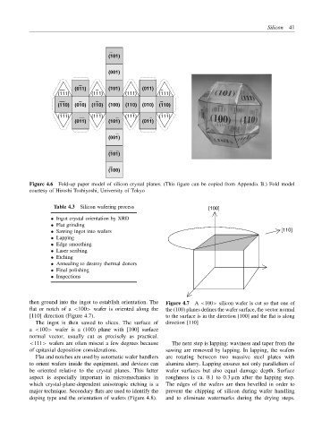
Figure 4.6 Fold-up paper model of silicon crystal planes. (This figure can be copied from Appendix B.) Fold model
courtesy of Hiroshi Toshiyoshi, University of Tokyo
Table 4.3 Silicon wafering process [100]
• Ingot crystal orientation by XRD
• Flat grinding
• Sawing ingot into wafers [110]
• Lapping
• Edge smoothing
• Laser scribing
• Etching
• Annealing to destroy thermal donors
• Final polishing
• Inspections
then ground into the ingot to establish orientation. The Figure 4.7 A <100> silicon wafer is cut so that one of
flat or notch of a <100> wafer is oriented along the the (100) planes defines the wafer surface, the vector normal
[110] direction (Figure 4.7). to the surface is in the direction [100] and the flat is along
The ingot is then sawed to slices. The surface of direction [110]
a <100> wafer is a (100) plane with [100] surface
normal vector, usually cut as precisely as practical.
<111> wafers are often miscut a few degrees because The next step is lapping: waviness and taper from the
of epitaxial deposition considerations. sawing are removed by lapping. In lapping, the wafers
Flat and notches are used by automatic wafer handlers are rotating between two massive steel plates with
to orient wafers inside the equipment, and devices can alumina slurry. Lapping ensures not only parallelism of
be oriented relative to the crystal planes. This latter wafer surfaces but also equal damage depth. Surface
aspect is especially important in micromechanics in roughness is ca. 0.1 to 0.3 µm after the lapping step.
which crystal-plane-dependent anisotropic etching is a The edges of the wafers are then bevelled in order to
major technique. Secondary flats are used to identify the prevent the chipping of silicon during wafer handling
doping type and the orientation of wafers (Figure 4.8). and to eliminate watermarks during the drying steps.