
Page 63 - Sami Franssila Introduction to Microfabrication
P. 63
42 Introduction to Microfabrication
(111) p-type (111) n-type (100) p-type (100) n-type (100) n-type
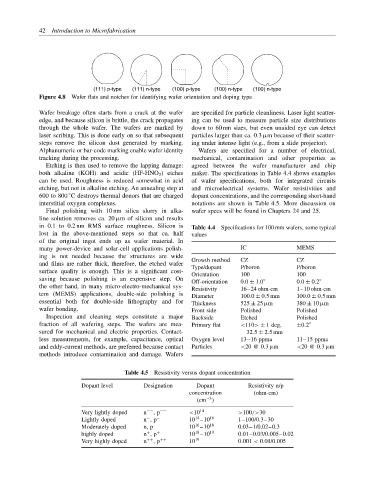
Figure 4.8 Wafer flats and notches for identifying wafer orientation and doping type
Wafer breakage often starts from a crack at the wafer are specified for particle cleanliness. Laser light scatter-
edge, and because silicon is brittle, the crack propagates ing can be used to measure particle size distributions
through the whole wafer. The wafers are marked by down to 60 nm sizes, but even unaided eye can detect
laser scribing. This is done early on so that subsequent particles larger than ca. 0.3 µm because of their scatter-
steps remove the silicon dust generated by marking. ing under intense light (e.g., from a slide projector).
Alphanumeric or bar-code marking enable wafer identity Wafers are specified for a number of electrical,
tracking during the processing. mechanical, contamination and other properties as
Etching is then used to remove the lapping damage: agreed between the wafer manufacturer and chip
both alkaline (KOH) and acidic (HF-HNO 3 ) etches maker. The specifications in Table 4.4 shows examples
can be used. Roughness is reduced somewhat in acid of wafer specifications, both for integrated circuits
etching, but not in alkaline etching. An annealing step at and microelectrical systems. Wafer resistivities and
◦
600 to 800 C destroys thermal donors that are charged dopant concentrations, and the corresponding short-hand
interstitial oxygen complexes. notations are shown in Table 4.5. More discussion on
Final polishing with 10 nm silica slurry in alka- wafer specs will be found in Chapters 24 and 25.
line solution removes ca. 20 µm of silicon and results
in 0.1 to 0.2 nm RMS surface roughness. Silicon is Table 4.4 Specifications for 100 mm wafers, some typical
lost in the above-mentioned steps so that ca. half values
of the original ingot ends up as wafer material. In
many power-device and solar-cell applications polish- IC MEMS
ing is not needed because the structures are wide
Growth method CZ CZ
and films are rather thick, therefore, the etched wafer
Type/dopant P/boron P/boron
surface quality is enough. This is a significant cost-
Orientation 100 100
saving because polishing is an expensive step. On ◦ ◦
Off-orientation 0.0 ± 1.0 0.0 ± 0.2
the other hand, in many micro-electro-mechanical sys-
Resistivity 16–24 ohm-cm 1–10 ohm-cm
tem (MEMS) applications, double-side polishing is Diameter 100.0 ± 0.5 mm 100.0 ± 0.5 mm
essential both for double-side lithography and for Thickness 525 ± 25 µm 380 ± 10 µm
wafer bonding. Front side Polished Polished
Inspection and cleaning steps constitute a major Backside Etched Polished
fraction of all wafering steps. The wafers are mea- Primary flat <110> ± 1 deg, ±0.2 ◦
sured for mechanical and electric properties. Contact- 32.5 ± 2.5 mm
less measurements, for example, capacitance, optical Oxygen level 13–16 ppma 11–15 ppma
and eddy-current methods, are preferred because contact Particles <20 @ 0.3 µm <20 @ 0.3 µm
methods introduce contamination and damage. Wafers
Table 4.5 Resistivity versus dopant concentration
Dopant level Designation Dopant Resistivity n/p
concentration (ohm-cm)
−3
(cm )
Very lightly doped n −− , p −− <10 14 >100/>30
14
−
Lightly doped n , p − 10 –10 16 1–100/0.3–30
16
Moderately doped n, p 10 –10 18 0.03–1/0.02–0.3
+
18
highly doped n , p + 10 –10 19 0.01–0.03/0.005–0.02
Very highly doped n ++ , p ++ 10 19 0.001 < 0.01/0.005