
Page 71 - Sami Franssila Introduction to Microfabrication
P. 71
50 Introduction to Microfabrication
science and technology, refer to Chapter 32). To get vapour pressure differences of the elements. Com-
uniform film thickness, the substrate direction relative to pound evaporation is also difficult because most com-
the beam is important, and substrate rotation is used to pounds do not evaporate as a molecular species, but
ensure uniformity. Uniformity is very much fixed when are decomposed. Some oxides (e.g., SiO 2 , B 2 O 3 ),
the chamber geometry is frozen, whereas in gas flow chalcogenides and halides do evaporate as molecules,
systems such as CVD, uniformity is very much process- and stoichiometric films can be obtained. The use
dependent. of multiple sources is a standard solution to multi-
Low melting-point metals, such as gold and alu- component films.
minium, can easily be evaporated, but refractory metals Evaporated metal films are usually under tensile
require more sophisticated heating methods. Localized stress, in the range of 100 MPa to 1 GPa. Non-
heating by an electron beam can vaporize even tungsten metals are found in both tensile and compressive
(melting point 3660 K), but deposition rates are, how- stresses, but the values are smaller than for metals.
ever, very low, of the order of angstroms per second. More discussion on thin-film stresses can be found in
Additionally, X-rays will be generated, which can dam- Chapter 7.
age sensitive devices.
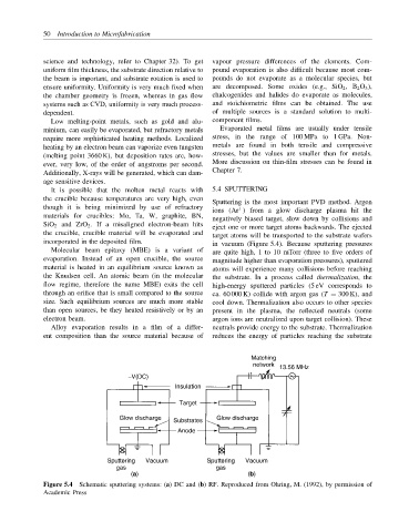
It is possible that the molten metal reacts with 5.4 SPUTTERING
the crucible because temperatures are very high, even Sputtering is the most important PVD method. Argon
though it is being minimized by use of refractory ions (Ar ) from a glow discharge plasma hit the
+
materials for crucibles: Mo, Ta, W, graphite, BN,
negatively biased target, slow down by collisions and
SiO 2 and ZrO 2 . If a misaligned electron-beam hits
eject one or more target atoms backwards. The ejected
the crucible, crucible material will be evaporated and target atoms will be transported to the substrate wafers
incorporated in the deposited film. in vacuum (Figure 5.4). Because sputtering pressures
Molecular beam epitaxy (MBE) is a variant of are quite high, 1 to 10 mTorr (three to five orders of
evaporation. Instead of an open crucible, the source magnitude higher than evaporation pressures), sputtered
material is heated in an equilibrium source known as atoms will experience many collisions before reaching
the Knudsen cell. An atomic beam (in the molecular the substrate. In a process called thermalization, the
flow regime, therefore the name MBE) exits the cell high-energy sputtered particles (5 eV corresponds to
through an orifice that is small compared to the source ca. 60 000 K) collide with argon gas (T = 300 K), and
size. Such equilibrium sources are much more stable cool down. Thermalization also occurs to other species
than open sources, be they heated resistively or by an present in the plasma, the reflected neutrals (some
electron beam. argon ions are neutralized upon target collision). These
Alloy evaporation results in a film of a differ- neutrals provide energy to the substrate. Thermalization
ent composition than the source material because of reduces the energy of particles reaching the substrate
Matching
network 13.56 MHz
−V(DC)
Insulation
Target
Glow discharge Substrates Glow discharge
Anode
Sputtering Vacuum Sputtering Vacuum
gas gas
(a) (b)
Figure 5.4 Schematic sputtering systems: (a) DC and (b) RF. Reproduced from Ohring, M. (1992), by permission of
Academic Press