
Page 76 - Sami Franssila Introduction to Microfabrication
P. 76
Thin-film Materials and Processes 55
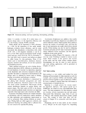
Figure 5.8 Damascene plating: seed layer sputtering; electroplating, polishing
where I is current, t is time, M is molar mass, n is Accelerators (brighteners) are additives that modify
species charge state, α is the deposition efficiency and the number of growth sites. Suppressors are additives for
F is the Faraday constant, 96 500 coulombs. surface diffusion control. Taken together, these additives
Noble metals can be deposited at 100% efficiency increase the number of nucleation sites, and keep the
(α = 1.00). In the deposition of less noble metals, size of each nucleation site small, which drives smooth
hydrogen evolution lowers efficiency, and for some growth. Pulsed plating can also be used in balancing
non-metals like phosphorus co-deposition with cobalt nucleation and grain growth: high overpotential and low
(Co:P, 12%, a soft magnetic material), α can be as surface diffusion favour nucleation, and the opposite
low as 0.20. Other typical electroplated metals include conditions favour grain growth.
nickel and iron–nickel (81% Ni, 19% Fe, Permalloy ). Damascene plating (Figure 5.8) deposits a film all
Tin–lead (40% lead in eutectic) and indium are plated over the wafer. Polishing is needed to remove excess
as solder bumps for chip packaging. Many of the metal. Metal remains in the grooves and recesses
metals used in microfabrication, aluminum, titanium, of the wafer, and the wafer surface remains planar.
tungsten, tantalum and niobium, do not have practical Electroplating can also be done in resist grooves,
electroplating processes. and more plating applications will be presented in
Three transport processes are active during electro- Chapters 23 and 27.
chemical deposition (ECD): diffusion at electrodes due
to local depletion of reactant via deposition, migration
5.6.3 Spin-coating
in the electrolyte and convective transport in the plat-
ing bath. The latter is connected to electrochemical cell Spin-coating is a very widely used method for resist
design, and it is affected by factors such as stirring, spinning and increasingly for other materials as well; for
heating, recirculation and hydrogen evolution. example, spin-on-glasses (SOGs) and thermally stable
Macroscopic current distribution is determined by polymers (known together as spin-on-dielectrics, SODs).
the plating bath electrode arrangement and wafer It is now a method to deposit films that will remain as
and bath conductivity. Electrical contact to the wafer structural parts of finished devices.
also needs careful consideration. Microscopic (local) Spinning is a simple process for viscous materi-
current distribution depends on pattern density and als deposition. Spinners, with typical speeds up to
pattern shapes. The third scale in ECD is the feature 10 000 rpm, are found in every microfabrication labo-
scale: potential gradients inside structures are important ratory. The main parameters for film thickness control
especially when high aspect ratio structures are filled. are viscosity, solvent evaporation rate and spin speed.
In practice, the plating solutions are complex mixtures Spin-coated film thicknesses range from 0.1 µm up
of electrolytes, salts for conductivity control, modifiers to 500 µm, with standard photoresists usually around
for film uniformity and morphology improvement as 1 µm. The coating of thick spin films will dis-
well as surfactants. Many plating solutions are propri- cussed in Chapter 10 in connection with thick photo-
etary. Plating baths are rather aggressive solutions, and resists.
photoresist leaching into plating bath or adhesion loss Dispensing can be in static mode, or slow rotation
are real concerns for reproducible plating. of ca. 300 rpm can be used (Figure 5.9). Depending