
Page 79 - Sami Franssila Introduction to Microfabrication
P. 79
58 Introduction to Microfabrication
Table 5.4 Properties of metals 5.8 DIELECTRIC THIN FILMS
Metal Resistivity CTE Thermal Melting Dielectric films have, just like metallic films, a plethora
◦
(µ -cm) (ppm/ C) conductivity point of applications in microdevices. The table below clas-
◦
(W/cm K) ( C) sifies dielectric film applications into three categories:
structural parts in finished devices, intermittent layers
Al 3 23 2.4 650
during wafer processing and protective coatings for fin-
Cu 1.7 16 4 1083
Mo 5.6 a 5 1.4 2610 ished devices. Surprisingly, many films can serve in all
W 5.6 a 4.5 1.7 3387 these roles.
Ta 12 a 6.5 0.6 3000
Ti 48 a 8.6 0.2 1660 Active, protective and sacrificial layers during wafer
Co 6.2 a 12.5 0.7 1500 processing
Ni 6.8 a 13 0.9 1455
Cr 13 a 6 0.7 1875 Mask for thermal Si 3 N 4
Pt 10 a 9 0.7 1769 oxidation
Au 1.7 14 3 1064 Diffusion and ion SiO 2 , Si 3 N 4
a Thin-film resistivity is much higher than bulk value: as a rule of thumb, implantation masks
1.5–2 times the bulk value can be used as an guestimate for thin-film Dopant evaporation barrier CVD oxide, SiN x
resistivity. Etch-stop layer in SiN x
polymer-based
inter-metal stacks
in solid. This correlation is seen in, for example, Window definition during CVD oxide
electromigration resistance. selective epitaxial
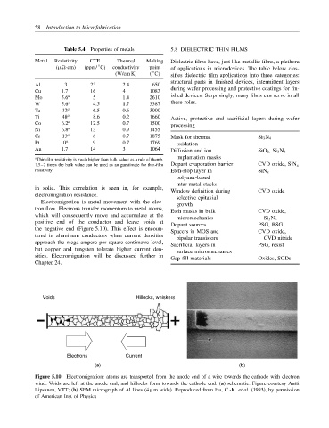
Electromigration is metal movement with the elec- growth
tron flow. Electrons transfer momentum to metal atoms, Etch masks in bulk CVD oxide,
which will consequently move and accumulate at the micromechanics
Si 3 N 4
positive end of the conductor and leave voids at Dopant sources PSG, BSG
the negative end (Figure 5.10). This effect is encoun- Spacers in MOS and CVD oxide,
tered in aluminum conductors when current densities bipolar transistors CVD nitride
approach the mega-ampere per square centimetre level, Sacrificial layers in PSG, resist
but copper and tungsten tolerate higher current den- surface micromechanics
sities. Electromigration will be discussed further in Gap fill materials Oxides, SODs
Chapter 24.
Voids Hillocks, whiskers
Electrons Current
(a) (b)
Figure 5.10 Electromigration: atoms are transported from the anode end of a wire towards the cathode with electron
wind. Voids are left at the anode end, and hillocks form towards the cathode end: (a) schematic. Figure courtesy Antti
Lipsanen, VTT; (b) SEM micrograph of Al lines (4 µm wide). Reproduced from Hu, C.-K. et al. (1993), by permission
of American Inst of Physics