
Page 82 - Sami Franssila Introduction to Microfabrication
P. 82
Thin-film Materials and Processes 61
benzo-cyclo-butadiene), photopatternable epoxy SU-8, and phase of reflected polarized light are measured.
polyimides (some of them photopatternable), fluorinated For very thin films (<10 nm) optical constants are not
poly(arylene ethers), fluoropolymer CPFP (cyclised really constants, and absolute accuracy of ellipsometry
perfluoro polymers like CYTOP ). is not very good, but precision is excellent. For thicker
PTFE, polytetrafluroethylene (Teflon is one variety films, multiple reflections and interference mean that
of PTFE) is also used, because of its special surface the solution is periodic, with the period given by
properties such as superhydrophobicity and extremely Equation 5.2:
low water absorption, <0.10% wt. Note that polymers
are sometimes used exactly because of their water λ 2 2
d = n − sin φ (5.2)
absorption: a capacitive humidity sensor measures the 2
change in the dielectric constant due to water absorption
in the polymer dielectric. Parylene (poly-para-xylylene) where φ is the angle of the incident laser beam and
is a versatile material that is strong enough mechanically λ, its wavelength. Measurement at two incident angles
◦
◦
so that released, free-standing structural parts can be (e.g., 50 and 70 ) gives additional information, and
made out of it. Parylene and CYTOP are exceptional period matching from the two measurements can give
polymers because they can tolerate KOH etching. thickness of layers. When film thickness is over 1 µm,
Parylene is deposited by CVD, whereas most other ellipsometry becomes difficult.
polymers are spin-coated. Ellipsometry needs a fairly large area for measure-
Polyimides offer some special properties: some ment, for example, 100 × 100 µm, while reflectometer
formulations are photopatternable like resists, and form spots can be as small as a few micrometres, which
permanent parts in finished devices. Some imides enables measurement from the structures themselves,
(PI2610) have coefficients of thermal expansion ca. without a dedicated test site. The easiest and quick-
3 ppm, close to silicon in the plane of the wafer, but est way to gauge thickness is from interference colours
◦
ca. 20 ppm/ C perpendicular to the surface. Thermal (Tables 5.6 and 5.7). The accuracy of this approach is
conductivities of imides are in the range 0.1 to 0.2 W/m ca. 10 nm, but the colours repeat at regular intervals,
K, an order of magnitude higher than that of silicon and absolute thickness determination requires additional
dioxide, but similar to that of silicon nitride. information.
Tensile strengths of polymers are in the range of 100
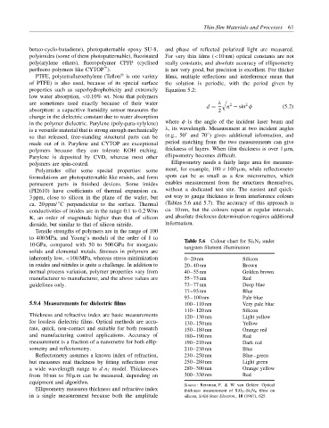
to 400 MPa, and Young’s moduli of the order of 1 to Table 5.6 Colour chart for Si 3 N 4 under
10 GPa, compared with 50 to 500 GPa for inorganic tungsten filament illumination
solids and elemental metals. Stresses in polymers are
inherently low, <100 MPa, whereas stress minimization 0–20 nm Silicon
in oxides and nitrides is quite a challenge. In addition to 20–40 nm Brown
normal process variation, polymer properties vary from 40–55 nm Golden brown
manufacturer to manufacturer, and the above values are 55–73 nm Red
guidelines only. 73–77 nm Deep blue
77–93 nm Blue
93–100 nm Pale blue
5.9.4 Measurements for dielectric films 100–110 nm Very pale blue
110–120 nm Silicon
Thickness and refractive index are basic measurements 120–130 nm Light yellow
for lossless dielectric films. Optical methods are accu- 130–150 nm Yellow
rate, quick, non-contact and suitable for both research 150–180 nm Orange red
and manufacturing control applications. Accuracy of 180–190 nm Red
measurement is a fraction of a nanometre for both ellip- 190–210 nm Dark red
sometry and reflectometry. 210–230 nm Blue
Reflectometry assumes a known index of refraction, 230–250 nm Blue–green
but measures real thickness by fitting reflections over 250–280 nm Light green
a wide wavelength range to d-n f model. Thicknesses 280–300 nm Orange yellow
from 10 nm to 50 µm can be measured, depending on 300–330 nm Red
equipment and algorithm. Source: Reizman, F. & W. van Gelder: Optical
Ellipsometry measures thickness and refractive index thickness measurement of SiO 2 –Si 3 N 4 films on
in a single measurement because both the amplitude silicon, Solid-State Electron., 10 (1967), 625.