
Page 85 - Sami Franssila Introduction to Microfabrication
P. 85
64 Introduction to Microfabrication
5.12 EXERCISES form electrical contact between gold electrodes).
Redrawn from Xue, M. et al. (2002).
1. Resistor design: How would you fabricate (a) 1 k ,
(b) 10 k resistors in a process in which minimum
linewidth is 3 µm? REFERENCES AND RELATED READINGS
2. Polysilicon sheet resistance is 50 /sq. What is Besser, R.S. et al: Chemical etch rate of plasma-enhanced
polysilicon thickness? chemical vapor deposited SiO 2 films, J. Electrochem. Soc.,
3. The DRAM memory cell is a capacitor. If the cell 144 (1997), 2859.
2
area is 1 µm , with a 4 nm oxide as the capacitor Cote, D.R. et al: Plasma-assisted chemical vapor deposition of
dielectric, and the operating voltage is 2 V, calculate dielectric thin films for ULSI semiconductor circuits, IBM J.
the number of electrons stored in the memory cell. Res. Dev., 43(1–2) (1999), 5.
4. The CVD oxide process is designed to target 500 nm Elshabini-Riad, A. & F.D. Barlow III: Thin Film Technology
thickness. If the wafers are violet, and the violet Handbook, McGraw-Hill, 1998.
changes to pink on wafer edges, what is repeatability Hu, C.-K. et al: Electromigration of Al(Cu) two-level struc-
tures: effect of Cu kinetics of damage formation, J. Appl.
and uniformity of this deposition process?
Phys., 74 (1993), 969.
5. If silane (SiH 4 ) flow in a single-wafer (150 mm) Jiles, D.C. & C.C.H. Lo: The role of new materials in the
3
PECVD reactor is 5 sccm (cm /min), what is
development of magnetic sensors and actuators, Sensors
the theoretical maximum deposition rate of amor- Actuators, 106 (2003), 3; special issue on magnetic sensors
phous silicon? and actuators.
6. If 20 nm of nickel reacts with overabundance of sili- Mahan, J.: Physical Vapor Deposition of Thin Films, Wiley,
con, how thick a layer of NiSi will be formed? Den- 2000.
3
3
3
sities: Si–2.3 g/cm , Ni–8.9 g/cm , NiSi–7.2 g/cm . Ohring, M.: The Materials Science of Thin Films, Academic
7. CoSi 2 is formed by cobalt thin-film reaction with Press, 1992.
silicon. What is the position of the CoSi 2 surface Pliskin, W. & E. Conrad: Non-destructive determination of
thickness and refractive index of transparent films, IBM J.
relative to the original silicon surface? Densities: Res. Dev., 1 (1964), 43.
3
3
Co–8.9 g/cm , CoSi 2 –5.3 g/cm . Reizman, F. & W. van Gelder: Optical thickness measurement
2
8. If ECD current density is 100 mA/cm , what will be of SiO 2 -Si 3 N 4 films on silicon, Solid-State Electron., 10
the nickel deposition rate? (1967), 625.
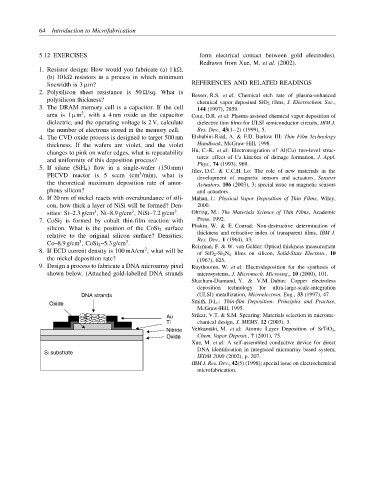
9. Design a process to fabricate a DNA microarray pixel Ruythooren, W. et al: Electrodeposition for the synthesis of
shown below. (Attached gold-labelled DNA strands microsystems, J. Micromech. Microeng., 10 (2000), 101.
Shacham-Diamand, Y. & V.M. Dubin: Copper electroless
deposition technology for ultra-large-scale-integration
DNA strands (ULSI) metallization, Microelectron. Eng., 33 (1997), 47.
Oxide Smith, D.L.: Thin-film Deposition: Principles and Practise,
McGraw-Hill, 1995.
Au Srikar, V.T. & S.M. Spearing: Materials selection in microme-
Ti chanical design, J. MEMS, 12 (2003), 3.
Nitride Vehkam¨ aki, M. et al: Atomic Layer Deposition of SrTiO 3 ,
Oxide Chem. Vapor Deposit., 7 (2001), 75.
Xue, M. et al: A self-assembled conductive device for direct
Si substrate DNA identification in integrated microarray based system,
IEDM 2000 (2002), p. 207.
IBM J. Res. Dev., 42(5) (1998); special issue on electrochemical
microfabrication.