
Page 90 - Sami Franssila Introduction to Microfabrication
P. 90
Epitaxy 69
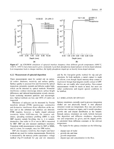
12:58:22 24-JAN-:3 19:11:20 24-MAI-:3
Boron
10 19 10 19 Phosphorus
Boron
10 18 Phosphorus 10 18
Phosphorus
Phosphorus 10 17
Concentration (cm −3 ) 10 16 Concentration (cm-3) 10 16
17
10
15
15
10
10
10 14 10 14
10 13 10 13
0.00 2.00 4.00 6.00 8.00 10.00 0.00 1.00 2.00 3.00 4.00 5.00 6.00
Depth (mm) Depth (mm)
(a) (b)
◦
Figure 6.7 (a) ICECREM simulation of epitaxial interface sharpness: three different growth temperatures (1050 C,
◦
◦
1100 C, 1150 C) have been used to grow a nominally 4 µm thick phosphorous doped epilayer on boron doped substrate.
Low temperature leads to sharper interface; (b) lightly phosphorus doped epi on heavily boron-doped substrate
6.2.2 Measurement of epitaxial deposition and by the four-point probe method for n/p and p/n
structures. In both methods, a metal contact is made
Three measurements must be carried out on epitax- on silicon, even though liquid mercury-drop contact is
ial wafers: thickness, resistivity and surface quality. much more benign than tungsten-needle contact of 4PP.
Surface quality is assessed first and foremost by optical Wafers are not usable after metal probes. Non-contact
inspection: pyramids, mounds and hillocks scatter light, measurements would be much in need, but most are
which can be detected by optical methods. Nomarski rather cumbersome and require special conditions to
interference contrast microscope detects surface height be fulfilled.
differences and infrared depolarization reveals stresses.
Laser scattering measures particles and microrough-
ness. Optical methods are fast, and 100% of wafers are 6.3 SIMULATION OF EPITAXY
inspected.
Thickness of epilayers can be measured by Fourier Epitaxy simulators currently used in process integration
transform infrared (FTIR) spectroscopy: constructive studies are not physically based. A true physical
and destructive interference from reflections at the sur- simulator would use temperature, flow rate and surface
face and at the substrate–epi interface are detected. reaction rate constants as inputs, and it would reproduce
FTIR requires, however, a highly doped substrate growth rate and dopant distribution as the outputs.
(resistivity below 0.025 ohm-cm). On resistive sub- Instead, epitaxy simulators are really hybrids between
strates, spreading resistance profiling (SRP) is used. film deposition and diffusion simulators: deposition
SRP requires sample bevelling, that is, it is sample- rate and temperature are given, and the dopant profile
destructive. One wafer in 25 or one in 100 is measured is calculated from diffusion constants at the relevant
by SRP. SRP can also measure multilayer structures. temperature.
Transition width measurement is done by SRP or SIMS, The inputs for the epitaxy simulator are the following:
and it is done, for example, once for 1000 wafers.
SRP also measures resistivity, but simpler and faster – dopant type of wafer
methods are used for routine measurements. Resistivity – growth rate and time
is measured by the mercury probe capacitance–voltage – growth temperature
method (Hg-CV-method) for p/p and n/n structures – dopant type and concentration in the flow.