
Page 91 - Sami Franssila Introduction to Microfabrication
P. 91
70 Introduction to Microfabrication
(a) (b) (c)
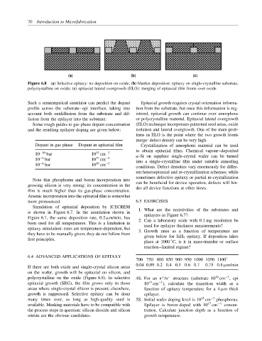
Figure 6.8 (a) Selective epitaxy: no deposition on oxide; (b) blanket deposition: epitaxy on single-crystalline substrate,
polycrystalline on oxide; (c) epitaxial lateral overgrowth (ELO): merging of epitaxial film fronts over oxide
Such a semiempirical simulator can predict the dopant Epitaxial growth requires crystal orientation informa-
profile across the substrate–epi interface, taking into tion from the substrate, but once this information is reg-
account both outdiffusion from the substrate and dif- istered, epitaxial growth can continue over amorphous
fusion from the epilayer into the substrate. or polycrystalline material. Epitaxial lateral overgrowth
Some rough guides to gas-phase dopant concentration (ELO) technique incorporates patterned seed areas, oxide
and the resulting epilayer doping are given below: isolation and lateral overgrowth. One of the main prob-
lems in ELO is the point where the two growth fronts
merge: defect density can be very high.
Dopant in gas phase Dopant in epitaxial film Crystallization of amorphous material can be used
to obtain epitaxial films. Chemical vapour–deposited
15
10 −10 bar 10 cm −3 α-Si on sapphire single-crystal wafer can be turned
17
10 −8 bar 10 cm −3 into a single-crystalline film under suitable annealing
19
10 −6 bar 10 cm −3
conditions. Defect densities vary enormously for differ-
ent heteroepitaxial and re-crystallization schemes; while
sometimes defective epitaxy or partial re-crystallization
Note that phosphorus and boron incorporation into
can be beneficial for device operation, defects will hin-
growing silicon is very strong: its concentration in the
der all device functions at other times.
film is much higher than its gas-phase concentration.
Arsenic incorporation into the epitaxial film is somewhat
more pronounced. 6.5 EXERCISES
Simulation of epitaxial deposition by ICECREM
1. What are the resistivities of the substrates and
is shown in Figure 6.7. In the simulation shown in
epilayers in Figure 6.7?
Figure 6.7, the same deposition rate, 0.2 µm/min, has
2. Can a laboratory scale with 0.1 mg resolution be
been used for all temperatures. This is a limitation in
used for epilayer thickness measurements?
epitaxy simulation: rates are temperature-dependent, but
3. Growth rates as a function of temperature are
they have to be manually given; they do not follow from
given below for SiH 4 epitaxy. If deposition takes
first principles. ◦
place at 1000 C, is it in mass-transfer or surface
reaction–limited regime?
6.4 ADVANCED APPLICATIONS OF EPITAXY ◦
700 750 800 850 900 950 1000 1050 1100
0.04 0.09 0.2 0.4 0.5 0.6 0.7 0.75 0.8 µm/min
If there are both oxide and single-crystal silicon areas
on the wafer, growth will be epitaxial on silicon, and
+
−3
18
polycrystalline on the oxide (Figure 6.8). In selective 4S. For an n /n − structure (substrate 10 cm , epi
15
epitaxial growth (SEG), the film grows only in those 10 cm ), calculate the transition width as a
−3
areas where single-crystal silicon is present; elsewhere, function of epitaxy temperature for a 4 µm thick
growth is suppressed. Selective epitaxy can be done epilayer.
15
many times over, as long as high-quality seed is 5S. Initial wafer doping level is 10 cm −3 phosphorus.
17
available. Masking materials have to be compatible with Epilayer is boron-doped with 10 cm −3 concen-
the process steps in question: silicon dioxide and silicon tration. Calculate junction depth as a function of
nitride are the obvious candidates. growth temperature.