
Page 96 - Sami Franssila Introduction to Microfabrication
P. 96
Thin-film Growth and Structure 75
(a) (b)
Figure 7.2 Thin-film growth modes: (a) 2D (layer-by-layer) and (b) 3D (island) growth. Early stage and coalescence
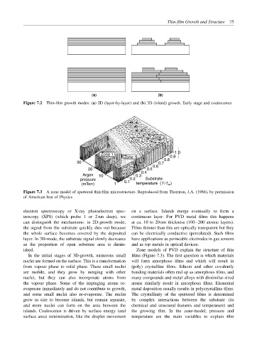
Zone 3
Zone 2
Zone 1 1.0
Zone 1 0.9
30 0.7 0.8
0.6
20 0.5
Argon 10 0.3 0.4
pressure 0.2 Substrate
(mTorr) 1 0.1 temperature (T/T )
m
Figure 7.3 A zone model of sputtered thin-film microstructure. Reproduced from Thornton, J.A. (1986), by permission
of American Inst of Physics
electron spectroscopy or X-ray photoelectron spec- on a surface. Islands merge eventually to form a
troscopy (XPS) (which probe 1 or 2 nm deep), we continuous layer. For PVD metal films this happens
can distinguish the mechanisms: in 2D-growth mode; at ca. 10 to 20 nm thickness (100–200 atomic layers).
the signal from the substrate quickly dies out because Films thinner than this are optically transparent but they
the whole surface becomes covered by the deposited can be electrically conductive (percolated). Such films
layer. In 3D-mode, the substrate signal slowly decreases have applications as permeable electrodes in gas sensors
as the proportion of open substrate area is dimin- and as top metals in optical devices.
ished. Zone models of PVD explain the structure of thin
In the initial stages of 3D-growth, numerous small films (Figure 7.3). The first question is which materials
nuclei are formed on the surface. This is a transformation will form amorphous films and which will result in
from vapour phase to solid phase. These small nuclei (poly) crystalline films. Silicon and other covalently
are mobile, and they grow by merging with other bonding materials often end up as amorphous films, and
nuclei, but they can also incorporate atoms from many compounds and metal alloys with dissimilar-sized
the vapour phase. Some of the impinging atoms re- atoms similarly result in amorphous films. Elemental
evaporate immediately and do not contribute to growth, metal deposition usually results in polycrystalline films.
and some small nuclei also re-evaporate. The nuclei The crystallinity of the sputtered films is determined
grow in size to become islands, but remain separate, by complex interactions between the substrate (its
and more nuclei can form on the area between the chemical and structural features and temperature) and
islands. Coalescence is driven by surface energy (and the growing film. In the zone-model, pressure and
surface area) minimization, like the droplet movement temperature are the main variables to explain film