
Page 101 - Sami Franssila Introduction to Microfabrication
P. 101
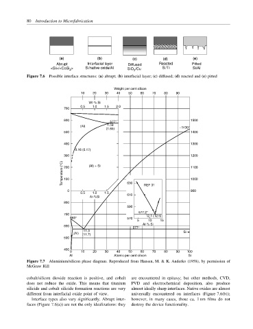
80 Introduction to Microfabrication


                          (a)             (b)            (c)          (d)          (e)
                         Abrupt       Interfacial layer  Diffused   Reacted       Pitted
                      <Si>/<CoSi >   Si/native oxide/Al   SiO /Cu     Si/Ti        Si/Al
                              2
                                                          2
            Figure 7.6 Possible interface structures: (a) abrupt; (b) interfacial layer; (c) diffused; (d) reacted and (e) pitted
                                                 Weight per cent silicon
                                   10   20   30   40   50   60   70    80   90

                                       Wt-% Si
                                   0.5  1.0  1.5  2.0
                            700
                            600                 577°                              1500
                                   (Al)       1.59
                                              (1.65)                         ∼1430°
                            500                                                   1400

                            400                                                   1300
                                 0.16 (0.17)
                            300                                                   1200
                           Temperature (°C)  200  (Al) + Si                       1100


                                                                                  1000
                            100
                              0                        630    REF 31              900
                                   0.5  1.0  1.5       610
                                       At-%Si
                            800
                                                       590
                                                            577.2°
                            700                                12.1 (12.5)
                               660°                    570
                                                           5    10   15
                                                             At-% Si
                            600                          577°
                                    11.3                                       Si
                                (Al)  (11.7)
                            500
                            400
                               0   10   20   30   40   50   60   70    80   90  100
                              Al                 Atomic per cent silicon         Si
            Figure 7.7 Aluminium/silicon phase diagram. Reproduced from Hansen, M. & K. Anderko (1958), by permission of
            McGraw Hill

            cobalt/silicon dioxide reaction is positive, and cobalt  are encountered in epitaxy; but other methods, CVD,
            does not reduce the oxide. This means that titanium  PVD and electrochemical deposition, also produce
            silicide and cobalt silicide formation reactions are very  almost ideally sharp interfaces. Native oxides are almost
            different from interfacial oxide point of view.  universally encountered on interfaces (Figure 7.6(b));
              Interface types also vary significantly. Abrupt inter-  however, in many cases, those ca. 1 nm films do not
            faces (Figure 7.6(a)) are not the only idealizations: they  destroy the device functionality.