
Page 103 - Sami Franssila Introduction to Microfabrication
P. 103
82 Introduction to Microfabrication
7.5.1 Measurement of adhesion layers and barriers 7.6 MULTILAYER FILMS
The first adhesion test is tape-pull test: adhesive tape
(standard office tape is commonly used) is attached to Performance of simple elemental or compound films,
the thin film and pulled off. If the film peels off with with or without barrier or adhesion layers, is often not
the tape, it has failed the adhesion test. More advanced enough, and multilayer films are introduced to offer
tests use a quantifiable pull force. improvement. Early integrated circuits used aluminium
Adhesion layer and diffusion-barrier stability can be for metallization. In order to improve interface stabil-
checked by electrical and physical measurements. Sheet- ity, Al-Si (1%) was adopted, and later TiW diffusion
resistance increase is a quick and simple measurement. barrier was added and Al-Si was replaced by Al-Si-Cu
for improved electromigration resistance. For many gen-
Copper resistivity is very low, 1.7 µohm-cm, and when
the barrier fails, the copper can react with the silicon erations, (0.8 − 0.5 − 0.35 − 0.25 µm) IC metallization
underneath, bringing about a resistance increase because was done with a Ti/TiN/Al/TiN film stack. Titanium acts
copper silicides CuSi and Cu 3 Si are high-resistivity as an adhesion promoter, TiN as a diffusion barrier, Al as
materials. They can be identified by X-ray diffraction, a current-carrying film and the top TiN has the dual role
but the resistance increase is indicative of silicide of mechanical stiffening of the structure and reflectiv-
formation. Pn-junction diode leakage is another quick ity reduction. Metallization reliability has been greatly
electrical measurement. improved by the adoption of such multilayer metalliza-
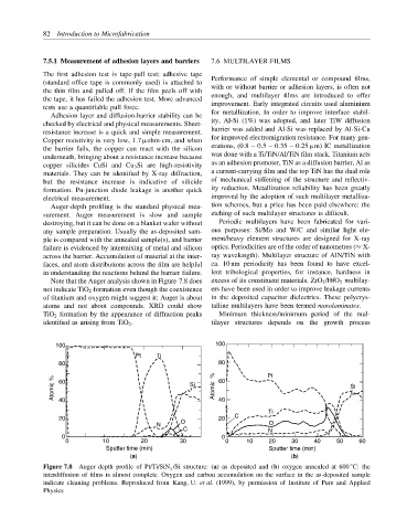
Auger-depth profiling is the standard physical mea- tion schemes, but a price has been paid elsewhere: the
surement. Auger measurement is slow and sample etching of such multilayer structures is difficult.
destroying, but it can be done on a blanket wafer without Periodic multilayers have been fabricated for vari-
any sample preparation. Usually the as-deposited sam- ous purposes: Si/Mo and W/C and similar light ele-
ple is compared with the annealed sample(s), and barrier ment/heavy element structures are designed for X-ray
failure is evidenced by intermixing of metal and silicon optics. Periodicities are of the order of nanometres (≈ X-
across the barrier. Accumulation of material at the inter- ray wavelength). Multilayer structure of AlN/TiN with
faces, and atom distributions across the film are helpful ca. 10 nm periodicity has been found to have excel-
in understanding the reactions behind the barrier failure. lent tribological properties, for instance, hardness in
Note that the Auger analysis shown in Figure 7.8 does excess of its constituent materials. ZrO 2 /HfO 2 multilay-
not indicate TiO 2 formation even though the coexistence ers have been used in order to improve leakage currents
of titanium and oxygen might suggest it: Auger is about in the deposited capacitor dielectrics. These polycrys-
atoms and not about compounds. XRD could show talline multilayers have been termed nanolaminates.
TiO 2 formation by the appearance of diffraction peaks Minimum thickness/minimum period of the mul-
identified as arising from TiO 2 . tilayer structures depends on the growth process
100 100
Pt Ti
80 80 Pt
Atomic % 60 Si Atomic % 60 Si
40
40
Ti
20 O 20 C
N O
C N
0 0
0 10 20 30 0 10 20 30 40 50 60
Sputter time (min) Sputter time (min)
(a) (b)
◦
Figure 7.8 Auger depth profile of Pt/Ti/SiN x /Si structure: (a) as deposited and (b) oxygen annealed at 600 C: the
interdiffusion of films is almost complete. Oxygen and carbon accumulation on the surface in the as-deposited sample
indicate cleaning problems. Reproduced from Kang, U. et al. (1999), by permission of Institute of Pure and Applied
Physics