
Page 104 - Sami Franssila Introduction to Microfabrication
P. 104
Thin-film Growth and Structure 83
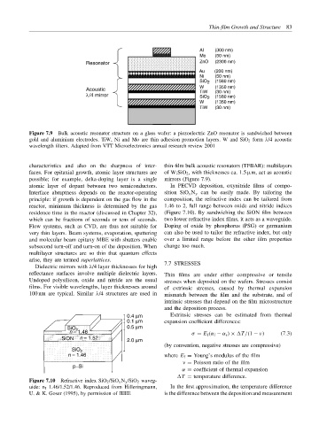
Al (300 nm)
Mo (50 nm)
Resonator ZnO (2300 nm)
Au (200 nm)
Ni (50 nm)
SiO 2 (1580 nm)
Acoustic W (1350 nm)
TiW
(30 nm)
λ/4 mirror SiO 2 (1580 nm)
W (1350 nm)
TiW (30 nm)
Figure 7.9 Bulk acoustic resonator structure on a glass wafer: a piezoelectric ZnO resonator is sandwiched between
gold and aluminium electrodes. TiW, Ni and Mo are thin adhesion promotion layers. W and SiO 2 form λ/4 acoustic
wavelength filters. Adapted from VTT Microelectronics annual research review 2001
characteristics and also on the sharpness of inter- thin-film bulk acoustic resonators (TFBAR): multilayers
faces. For epitaxial growth, atomic layer structures are of W:SiO 2 , with thicknesses ca. 1.5 µm, act as acoustic
possible; for example, delta-doping layer is a single mirrors (Figure 7.9).
atomic layer of dopant between two semiconductors. In PECVD deposition, oxynitride films of compo-
Interface abruptness depends on the reactor-operating sition SiO x N y can be easily made. By tailoring the
principle: if growth is dependent on the gas flow in the composition, the refractive index can be tailored from
reactor, minimum thickness is determined by the gas 1.46 to 2, full range between oxide and nitride indices
residence time in the reactor (discussed in Chapter 32), (Figure 7.10). By sandwiching the SiON film between
which can be fractions of seconds or tens of seconds. two lower refractive index films, it acts as a waveguide.
Flow systems, such as CVD, are thus not suitable for Doping of oxide by phosphorus (PSG) or germanium
very thin layers. Beam systems, evaporation, sputtering can also be used to tailor the refractive index, but only
and molecular beam epitaxy MBE with shutters enable over a limited range before the other film properties
subsecond turn-off and turn-on of the deposition. When change too much.
multilayer structures are so thin that quantum effects
arise, they are termed superlattices.
Dielectric mirrors with λ/4 layer thicknesses for high 7.7 STRESSES
reflectance surfaces involve multiple dielectric layers. Thin films are under either compressive or tensile
Undoped polysilicon, oxide and nitride are the usual stresses when deposited on the wafers. Stresses consist
films. For visible wavelengths, layer thicknesses around of extrinsic stresses, caused by thermal expansion
100 nm are typical. Similar λ/4 structures are used in mismatch between the film and the substrate, and of
intrinsic stresses that depend on the film microstructure
and the deposition process.
0.4 µm Extrinsic stresses can be estimated from thermal
0.1 µm expansion coefficient differences:
SiO 2 0.5 µm
n = 1.46 σ = E f (α f − α s ) × T/(1 − ν) (7.3)
SiON n = 1.52 2.0 µm
(by convention, negative stresses are compressive)
SiO 2
n = 1.46 where E f = Young’s modulus of the film
ν = Poisson ratio of the film
p−Si
α = coefficient of thermal expansion
T = temperature difference.
Figure 7.10 Refractive index SiO 2 /SiO x N y /SiO 2 waveg-
uide: n f 1.46/1.52/1.46. Reproduced from Hilleringmann, In the first approximation, the temperature difference
U. & K. Goser (1995), by permission of IEEE is the difference between the deposition and measurement