
Page 107 - Sami Franssila Introduction to Microfabrication
P. 107
86 Introduction to Microfabrication
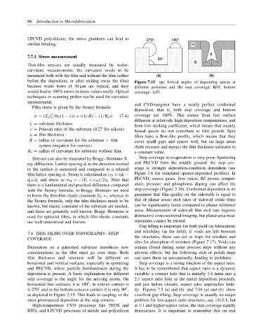
LPCVD polysilicon), the stress gradients can lead to 270° 180°
similar bending. H
A
7.7.1 Stress measurement
90°
B
Thin-film stresses are usually measured by wafer-
curvature measurements: the curvature needs to be
measured both with the film and without the film (either (a) (b)
before the deposition; or after etching away the film) Figure 7.15 (a) Arrival angles of depositing specie at
because wafer bows of 30 µm are typical, and they different positions and (b) step coverage: B/H; bottom
would lead to 100% errors in stress values easily. Optical coverage: A/H
techniques or scanning probes can be used for curvature
measurement.
Film stress is given by the Stoney formula: and CVD-tungsten have a nearly perfect conformal
deposition, that is, both step coverage and bottom
2
σ = (E s t /6t f (1 − ν)) × ((1/R) − (1/R 0 )) (7.4) coverage are 100%. This comes from fast surface
s
diffusion at relatively high deposition temperatures, and
t s = substrate thickness
from low-sticking coefficient, which means that weakly
ν = Poisson ratio of the substrate (0.27 for silicon) bound specie do not contribute to film growth. Spin
t f = film thickness films have a flow-like profile, which means that they
R = radius of curvature for the substrate + film cover small gaps and spaces well, but on large areas
system (negative for convex) (both recesses and mesas) the film thickness saturates to
R 0 = radius of curvature for substrate without film. a constant value.
Stresses can also be measured by Bragg–Brentano X- Step coverage in evaporation is very poor. Sputtering
ray diffraction. Lattice spacing d f in the direction normal and PECVD form the middle ground: the step cov-
to the surface is measured and compared to a relaxed erage is strongly deposition-condition dependent (see
film lattice spacing d r . Strain is calculated as ε 33 = (d f − Figure 3.6 for simulated sputter-deposited profiles). In
d r )/d r and stress as σ 11 = −(E f × ε 33 )/2ν f . Note that PECVD, source gases, flow ratios, RF power, temper-
there is a fundamental and practical difference compared ature, pressure and phosphorus doping can affect the
with the Stoney formula: in Bragg–Brentano we need step coverage (Figure 7.16). Conformal deposition is no
to know the thin-film elastic constants E f , ν f , whereas in guarantee that film quality on the sidewalls is equal to
the Stoney formula, only the film thickness needs to be that of planar areas: etch rates of sidewall oxide films
known, but elastic constants of the substrate are needed, can be significantly faster compared to planar reference
and these are generally well known. Bragg–Brentano is areas. Measurement of sidewall film etch rate requires
used for epitaxial films, in which film elastic constants destructive cross-sectional imaging, but planar area mea-
are well understood and known. surements cannot be trusted.
Gap filling is important for both yield (in fabrication)
and reliability (in the field): if voids are left between
7.8 THIN FILMS OVER TOPOGRAPHY: STEP
COVERAGE the structures, these can act as traps for residues and
sites for absorption of moisture (Figure 7.17). Voids can
Deposition on a patterned substrate introduces new remain closed during some process steps without any
considerations as the film must go over steps. Both adverse effects, but the following etch or polish steps
film thickness and structure will be different on can open them up unexpectedly, leading to problems.
horizontal and vertical surfaces, especially in sputtering Step coverage is a strong function of the aspect ratio.
and PECVD, where particle bombardment during the It has to be remembered that aspect ratio is a dynamic
deposition is present. A basic explanation for different variable: a contact hole that is initially 1:1 turns into a
step coverage is the angle for the arriving atoms. On 2:1 aspect ratio hole as the metal deposition proceeds,
horizontal free surfaces, it is 180 , in convex corners it and just before closure, aspect ratio approaches infin-
◦
◦
is 270 and in the bottom concave corners it is only 90 , ity. Figures 7.5 (a) and (b) and 7.16 (a) and (b) show
◦
as depicted in Figure 7.15. This leads to cusping, or the excellent gap filling. Step coverage is usually no major
most pronounced deposition at the step corners. problem for low-aspect ratio structures, say <0.5:1, but
High-temperature CVD processes like TEOS and at 1:1 and higher-aspect ratios, the step coverage rapidly
HTO, and LPCVD processes of nitride and polysilicon deteriorates. It is important to remember that on real